Report an Error


NVIDIA GeForce GT 730
- Graphics Processor
- GK208B
- Cores
- 384
- TMUs
- 32
- ROPs
- 8
- Memory Size
- 1024 MB
- Memory Type
- GDDR5
- Bus Width
- 64 bit

GPU

Bottom
Recommended Gaming Resolutions:
- 1366x768
- 1600x900
- 1920x1080
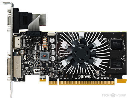
The GeForce GT 730 was a graphics card by NVIDIA, launched on June 18th, 2014. Built on the 28 nm process, and based on the GK208B graphics processor, in its GK208-302-B1 variant, the card supports DirectX 12. Even though it supports DirectX 12, the feature level is only 11_0, which can be problematic with newer DirectX 12 titles. The GK208B graphics processor is a relatively small chip with a die area of only 87 mm² and 1,020 million transistors. It features 384 shading units, 32 texture mapping units, and 8 ROPs. NVIDIA has paired 1,024 MB GDDR5 memory with the GeForce GT 730, which are connected using a 64-bit memory interface. The GPU is operating at a frequency of 902 MHz, memory is running at 1253 MHz (5 Gbps effective).
Being a single-slot card, the NVIDIA GeForce GT 730 does not require any additional power connector, its power draw is rated at 38 W maximum. Display outputs include: 1x DVI, 1x HDMI 1.4a, 1x VGA. GeForce GT 730 is connected to the rest of the system using a PCI-Express 2.0 x8 interface. The card measures 145 mm in length, and features a single-slot cooling solution.
Being a single-slot card, the NVIDIA GeForce GT 730 does not require any additional power connector, its power draw is rated at 38 W maximum. Display outputs include: 1x DVI, 1x HDMI 1.4a, 1x VGA. GeForce GT 730 is connected to the rest of the system using a PCI-Express 2.0 x8 interface. The card measures 145 mm in length, and features a single-slot cooling solution.
Graphics Processor
- GPU Name
- GK208B
- GPU Variant
- GK208-302-B1
- Architecture
- Kepler 2.0
- Foundry
- TSMC
- Process Size
- 28 nm
- Transistors
- 1,020 million
- Density
- 11.7M / mm²
- Die Size
- 87 mm²
- Chip Package
- FCBGA-595
Graphics Card
- Release Date
- Jun 18th, 2014
- Generation
- GeForce 700
- Predecessor
- GeForce 600
- Successor
- GeForce 900
- Production
- End-of-life
- Bus Interface
- PCIe 2.0 x8
Clock Speeds
- GPU Clock
- 902 MHz
- Memory Clock
-
1253 MHz
5 Gbps effective
Memory
- Memory Size
- 1024 MB
- Memory Type
- GDDR5
- Memory Bus
- 64 bit
- Bandwidth
- 40.10 GB/s
Render Config
- Shading Units
- 384
- TMUs
- 32
- ROPs
- 8
- SMX Count
- 2
- L1 Cache
- 16 KB (per SMX)
- L2 Cache
- 512 KB
Theoretical Performance
- Pixel Rate
- 7.216 GPixel/s
- Texture Rate
- 28.86 GTexel/s
- FP32 (float)
- 692.7 GFLOPS
- FP64 (double)
- 28.86 GFLOPS (1:24)
Board Design
- Slot Width
- Single-slot
- Length
- 145 mm
5.7 inches
- TDP
- 38 W
- Suggested PSU
- 200 W
- Outputs
- 1x DVI
1x HDMI 1.4a
1x VGA
- Power Connectors
- None
- Board Number
- P2131 SKU 10,
P2132 SKU 10
Graphics Features
- DirectX
- 12 (11_0)
- OpenGL
- 4.6
- OpenCL
- 3.0
- Vulkan
- 1.2.175
- CUDA
- 3.5
- Shader Model
- 6.5 (5.1)
GK208B GPU Notes
| NVENC: No Support NVDEC: 1st Gen PureVideo HD: VP5 VDPAU: Feature Set D L1 Cache is configurable from 16 KB up to 48 KB per SMX |
Retail boards based on this design (15)
| Name | GPU Clock | Memory Clock | Other Changes |
|---|---|---|---|
| 902 MHz | 1253 MHz | 2 GB, 150 mm/5.9 inches | |
| 902 MHz | 900 MHz | 2 GB, DDR3 | |
| 902 MHz | 800 MHz | 2 GB, DDR3, 137 mm/5.4 inches | |
| 902 MHz | 1253 MHz | 2 GB | |
| 902 MHz | 900 MHz | 2 GB, DDR3 | |
| 902 MHz | 1253 MHz | ||
| 902 MHz | 1253 MHz | 2 GB | |
| 902 MHz | 1253 MHz | 2 GB, 177 mm/7 inches | |
| 902 MHz | 800 MHz | 2 GB, DDR3, 177 mm/7 inches | |
| 1006 MHz | 1253 MHz | 178 mm/7 inches | |
| 902 MHz | 1253 MHz | 2 GB, 144 mm/5.7 inches | |
| 902 MHz | 900 MHz | 2 GB, DDR3, 165 mm/6.5 inches, 2x DisplayPort | |
| 902 MHz | 1253 MHz | ||
| 1006 MHz | 1253 MHz | 141 mm/5.6 inches | |
| 1006 MHz | 1253 MHz | 2 GB, 141 mm/5.6 inches |


Apr 18th, 2024 05:20 EDT
change timezone
Latest GPU Drivers
New Forum Posts
- Will a RTX 4070 TI super bottleneck a Ryzen 9 7950X3D? (31)
- Issue of the RTX 4050's L2 Cache in the Techpowerup GPU Database (0)
- Which air cooler for a ryzen 9 5900x (153)
- Realtek Modded Audio Driver for Windows 10/11 - Only for HDAUDIO (5676)
- Post your JetStream 2 speeds! (140)
- The TPU UK Clubhouse (24725)
- Unlocked Realtek HD Audio Drivers for Windows 11 (Dolby Digital Live/DTS Interactive) (150)
- Sold my a working PSU that I have been using, but buyer says it sparked at the outlet when he plugged it in and asking for a possible refund (9)
- Gigabyte gpu model differences? (30)
- Identify my GPU - RX 570 8GB (or what?) (1)
Popular Reviews
- Horizon Forbidden West Performance Benchmark Review - 30 GPUs Tested
- PowerColor Radeon RX 7900 GRE Hellhound Review
- ASUS GeForce RTX 4090 Matrix Platinum Review - The RTX 4090 Ti
- Fractal Design Terra Review
- Corsair 2000D Airflow Review
- Minisforum EliteMini UM780 XTX (AMD Ryzen 7 7840HS) Review
- Creative Pebble X Plus Review
- FiiO KB3 HiFi Mechanical Keyboard Review - Integrated DAC/Amp!
- ASUS GeForce RTX 4090 STRIX OC Review
- NVIDIA GeForce RTX 4090 Founders Edition Review - Impressive Performance
Controversial News Posts
- Sony PlayStation 5 Pro Specifications Confirmed, Console Arrives Before Holidays (106)
- NVIDIA Points Intel Raptor Lake CPU Users to Get Help from Intel Amid System Instability Issues (102)
- US Government Wants Nuclear Plants to Offload AI Data Center Expansion (98)
- Windows 10 Security Updates to Cost $61 After 2025, $427 by 2028 (82)
- Developers of Outpost Infinity Siege Recommend Underclocking i9-13900K and i9-14900K for Stability on Machines with RTX 4090 (82)
- TechPowerUp Hiring: Reviewers Wanted for Motherboards, Laptops, Gaming Handhelds and Prebuilt Desktops (71)
- Intel Realizes the Only Way to Save x86 is to Democratize it, Reopens x86 IP Licensing (70)
- AMD Zen 5 Execution Engine Leaked, Features True 512-bit FPU (63)