Report an Error


NVIDIA GeForce GTX 550 Ti
- Graphics Processor
- GF116
- Cores
- 192
- TMUs
- 32
- ROPs
- 24
- Memory Size
- 1024 MB
- Memory Type
- GDDR5
- Bus Width
- 192 bit


GPU
I/O
Recommended Gaming Resolutions:
- 1366x768
- 1600x900
- 1920x1080
The GeForce GTX 550 Ti was a mid-range graphics card by NVIDIA, launched on March 15th, 2011. Built on the 40 nm process, and based on the GF116 graphics processor, in its GF116-400-A1 variant, the card supports DirectX 12. Even though it supports DirectX 12, the feature level is only 11_0, which can be problematic with newer DirectX 12 titles. The GF116 graphics processor is an average sized chip with a die area of 238 mm² and 1,170 million transistors. It features 192 shading units, 32 texture mapping units, and 24 ROPs. NVIDIA has paired 1,024 MB GDDR5 memory with the GeForce GTX 550 Ti, which are connected using a 192-bit memory interface. The GPU is operating at a frequency of 900 MHz, memory is running at 1026 MHz (4.1 Gbps effective).
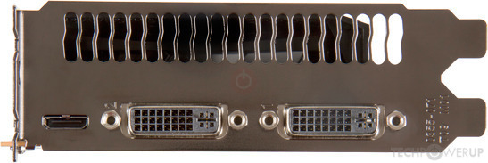
Being a dual-slot card, the NVIDIA GeForce GTX 550 Ti draws power from 1x 6-pin power connector, with power draw rated at 116 W maximum. Display outputs include: 2x DVI, 1x mini-HDMI 1.3a. GeForce GTX 550 Ti is connected to the rest of the system using a PCI-Express 2.0 x16 interface. The card measures 210 mm in length, and features a dual-slot cooling solution. Its price at launch was 149 US Dollars.
Being a dual-slot card, the NVIDIA GeForce GTX 550 Ti draws power from 1x 6-pin power connector, with power draw rated at 116 W maximum. Display outputs include: 2x DVI, 1x mini-HDMI 1.3a. GeForce GTX 550 Ti is connected to the rest of the system using a PCI-Express 2.0 x16 interface. The card measures 210 mm in length, and features a dual-slot cooling solution. Its price at launch was 149 US Dollars.
Graphics Processor
Graphics Card
- Release Date
- Mar 15th, 2011
- Generation
- GeForce 500
- Predecessor
- GeForce 400
- Successor
- GeForce 600
- Production
- End-of-life
- Launch Price
- 149 USD
- Bus Interface
- PCIe 2.0 x16
- Reviews
- 62 in our database
Relative Performance
Based on TPU review data: "Performance Summary" at 1920x1080, 4K for 2080 Ti and faster.
Clock Speeds
- GPU Clock
- 900 MHz
- Shader Clock
- 1800 MHz
- Memory Clock
-
1026 MHz
4.1 Gbps effective
Memory
- Memory Size
- 1024 MB
- Memory Type
- GDDR5
- Memory Bus
- 192 bit
- Bandwidth
- 98.50 GB/s
Render Config
- Shading Units
- 192
- TMUs
- 32
- ROPs
- 24
- SM Count
- 4
- L1 Cache
- 64 KB (per SM)
- L2 Cache
- 384 KB
Theoretical Performance
- Pixel Rate
- 7.200 GPixel/s
- Texture Rate
- 28.80 GTexel/s
- FP32 (float)
- 691.2 GFLOPS
- FP64 (double)
- 57.60 GFLOPS (1:12)
Board Design
- Slot Width
- Dual-slot
- Length
- 210 mm
8.3 inches
- TDP
- 116 W
- Suggested PSU
- 300 W
- Outputs
- 2x DVI
1x mini-HDMI 1.3a
- Power Connectors
- 1x 6-pin
- Board Number
- P1050 SKU 0
Graphics Features
- DirectX
- 12 (11_0)
- OpenGL
- 4.6
- OpenCL
- 1.1
- Vulkan
- N/A
- CUDA
- 2.1
- Shader Model
- 5.1
GF116 GPU Notes
| PureVideo HD: VP4 VDPAU: Feature Set C |
Retail boards based on this design (20)
| Name | GPU Clock | Memory Clock | Other Changes |
|---|---|---|---|
| 910 MHz | 1026 MHz | 1x DVI 1x HDMI 1x VGA | |
| 975 MHz | 1026 MHz | 230 mm/9.1 inches, 1x DVI 1x HDMI 1x VGA | |
| 1015 MHz | 1050 MHz | 230 mm/9.1 inches, 1x DVI 1x HDMI 1x VGA | |
| 950 MHz | 1075 MHz | 2 GB, 250 mm/9.8 inches | |
| 1000 MHz | 1100 MHz | 250 mm/9.8 inches | |
| 900 MHz | 1026 MHz | Single-slot | |
| 900 MHz | 1002 MHz | 2 GB | |
| 972 MHz | 1128 MHz | ||
| 972 MHz | 1026 MHz | 2 GB | |
| 952 MHz | 1089 MHz | ||
| 981 MHz | 1128 MHz | ||
| 1000 MHz | 1100 MHz | 190 mm/7.5 inches, 1x DVI 1x HDMI 1x VGA | |
| 970 MHz | 1026 MHz | 226 mm/8.9 inches | |
| 970 MHz | 1026 MHz | 239 mm/9.4 inches, Single-slot, 1x DVI 1x HDMI 1x VGA | |
| 1000 MHz | 1150 MHz | 1x DVI 1x HDMI 1x DisplayPort | |
| 900 MHz | 1026 MHz | ||
| 780 MHz | 940 MHz | 1x DVI 1x HDMI 1x VGA | |
| 1000 MHz | 1200 MHz | ||
| 950 MHz | 1100 MHz | ||
| 1000 MHz | 1100 MHz | 188 mm/7.4 inches, 2x DVI 1x HDMI 1x DisplayPort |


Apr 23rd, 2024 17:26 EDT
change timezone
Latest GPU Drivers
New Forum Posts
- What's your latest tech purchase? (20301)
- ThrottleStop 9.6 Voltage won't change (1)
- need help with motherboard/ ram compability certainty (9)
- FINAL FANTASY XIV: Dawntrail Official Benchmark (71)
- CPB Enabled Boot Loop (8)
- No POST, and no display (8)
- Aida64 cache mem OC (5)
- hacked (72)
- Meta Horizon OS (6)
- windows 11 (4)
Popular Reviews
- Horizon Forbidden West Performance Benchmark Review - 30 GPUs Tested
- Fractal Design Terra Review
- Corsair 2000D Airflow Review
- Thermalright Phantom Spirit 120 EVO Review
- Minisforum EliteMini UM780 XTX (AMD Ryzen 7 7840HS) Review
- ASUS GeForce RTX 4090 STRIX OC Review
- NVIDIA GeForce RTX 4090 Founders Edition Review - Impressive Performance
- ASUS GeForce RTX 4090 Matrix Platinum Review - The RTX 4090 Ti
- Creative Pebble X Plus Review
- MSI GeForce RTX 4090 Gaming X Trio Review
Controversial News Posts
- Sony PlayStation 5 Pro Specifications Confirmed, Console Arrives Before Holidays (116)
- NVIDIA Points Intel Raptor Lake CPU Users to Get Help from Intel Amid System Instability Issues (106)
- AMD "Strix Halo" Zen 5 Mobile Processor Pictured: Chiplet-based, Uses 256-bit LPDDR5X (101)
- US Government Wants Nuclear Plants to Offload AI Data Center Expansion (98)
- Windows 10 Security Updates to Cost $61 After 2025, $427 by 2028 (84)
- Developers of Outpost Infinity Siege Recommend Underclocking i9-13900K and i9-14900K for Stability on Machines with RTX 4090 (84)
- TechPowerUp Hiring: Reviewers Wanted for Motherboards, Laptops, Gaming Handhelds and Prebuilt Desktops (74)
- Intel Realizes the Only Way to Save x86 is to Democratize it, Reopens x86 IP Licensing (70)