Report an Error


HIS HD 4830 Single Slot
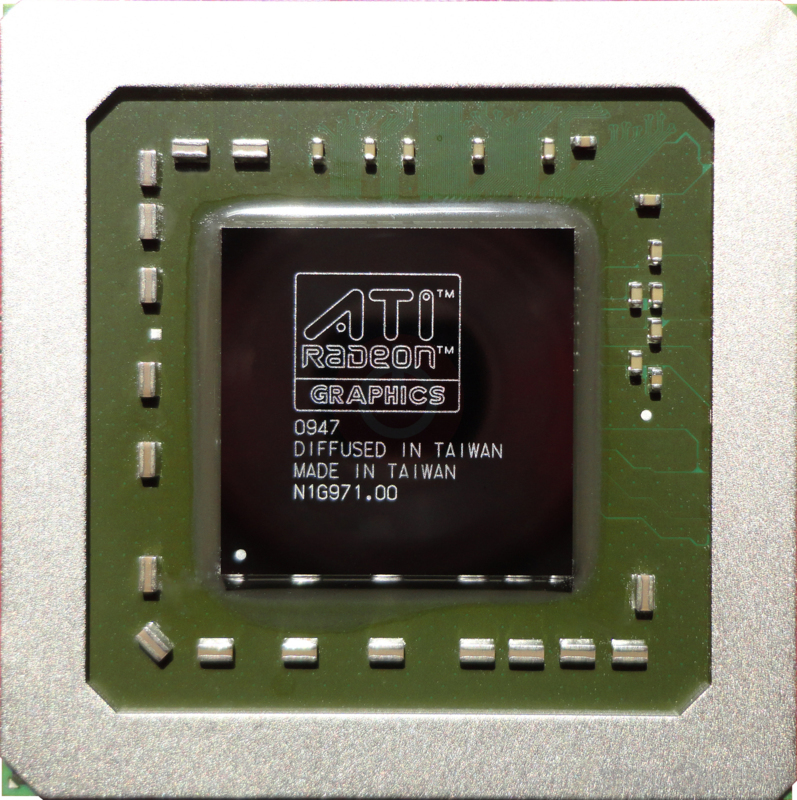
- Graphics Processor
- RV770
- Cores
- 640
- TMUs
- 32
- ROPs
- 16
- Memory Size
- 512 MB
- Memory Type
- GDDR3
- Bus Width
- 256 bit

GPU

Rear

Back
Graphics Processor
Graphics Card
- Release Date
- Oct 21st, 2008
- Generation
-
Radeon R700
(HD 4800)
- Predecessor
- Radeon R600
- Successor
- Evergreen
- Production
- End-of-life
- Bus Interface
- PCIe 2.0 x16
Clock Speeds
- GPU Clock
- 575 MHz
- Memory Clock
-
900 MHz
1800 Mbps effective
Memory
- Memory Size
- 512 MB
- Memory Type
- GDDR3
- Memory Bus
- 256 bit
- Bandwidth
- 57.60 GB/s
Render Config
- Shading Units
- 640
- TMUs
- 32
- ROPs
- 16
- Compute Units
- 8
- L1 Cache
- 16 KB (per CU)
- L2 Cache
- 256 KB
Theoretical Performance
- Pixel Rate
- 9.200 GPixel/s
- Texture Rate
- 18.40 GTexel/s
- FP32 (float)
- 736.0 GFLOPS
- FP64 (double)
- 147.2 GFLOPS (1:5)
Board Design
- Slot Width
- Single-slot
- Length
- 246 mm
9.7 inches
- Width
- 111 mm
4.4 inches
- Height
- 20 mm
0.8 inches
- TDP
- 95 W
- Suggested PSU
- 250 W
- Outputs
- 2x DVI
1x S-Video
- Power Connectors
- 1x 6-pin
- Board Number
- 109-B50131-10
Graphics Features
- DirectX
- 10.1 (10_1)
- OpenGL
- 3.3
- OpenCL
- 1.1
- Vulkan
- N/A
- Shader Model
- 4.1
RV770 GPU Notes
| Mobile Variant: M98 Codename: Wekiva Graphics/Compute: GFX3 Display Core Engine: 3.1 Unified Video Decoder: 2.0 |
Other retail boards based on this design (1)
| Name | GPU Clock | Memory Clock | Other Changes |
|---|---|---|---|
|
HIS HD 4830 Single Slot

|
575 MHz | 900 MHz |
Apr 23rd, 2024 14:04 EDT
change timezone
Latest GPU Drivers
New Forum Posts
- No POST, and no display (2)
- Shadow Of The Tomb Raider - CPU Performance and general game benchmark discussions (524)
- Drop fps (3)
- Embracer Group is breaking into 3 smaller companies... lol who saw this coming, what a joke (9)
- FINAL FANTASY XIV: Dawntrail Official Benchmark (69)
- Which new games will you be buying? (296)
- DTS DCH Driver for Realtek HDA [DTS:X APO4 + DTS Interactive] (1908)
- Is there a technical reason that Windows 11 doesn't have built into it battery charge limitation? (34)
- hacked (71)
- after hack (3)
Popular Reviews
- Horizon Forbidden West Performance Benchmark Review - 30 GPUs Tested
- Fractal Design Terra Review
- Corsair 2000D Airflow Review
- Thermalright Phantom Spirit 120 EVO Review
- Minisforum EliteMini UM780 XTX (AMD Ryzen 7 7840HS) Review
- ASUS GeForce RTX 4090 STRIX OC Review
- NVIDIA GeForce RTX 4090 Founders Edition Review - Impressive Performance
- ASUS GeForce RTX 4090 Matrix Platinum Review - The RTX 4090 Ti
- Creative Pebble X Plus Review
- MSI GeForce RTX 4090 Gaming X Trio Review
Controversial News Posts
- Sony PlayStation 5 Pro Specifications Confirmed, Console Arrives Before Holidays (116)
- NVIDIA Points Intel Raptor Lake CPU Users to Get Help from Intel Amid System Instability Issues (105)
- AMD "Strix Halo" Zen 5 Mobile Processor Pictured: Chiplet-based, Uses 256-bit LPDDR5X (101)
- US Government Wants Nuclear Plants to Offload AI Data Center Expansion (98)
- Windows 10 Security Updates to Cost $61 After 2025, $427 by 2028 (84)
- Developers of Outpost Infinity Siege Recommend Underclocking i9-13900K and i9-14900K for Stability on Machines with RTX 4090 (83)
- TechPowerUp Hiring: Reviewers Wanted for Motherboards, Laptops, Gaming Handhelds and Prebuilt Desktops (74)
- Intel Realizes the Only Way to Save x86 is to Democratize it, Reopens x86 IP Licensing (70)