Report an Error


HP HD 7670M 2 GB
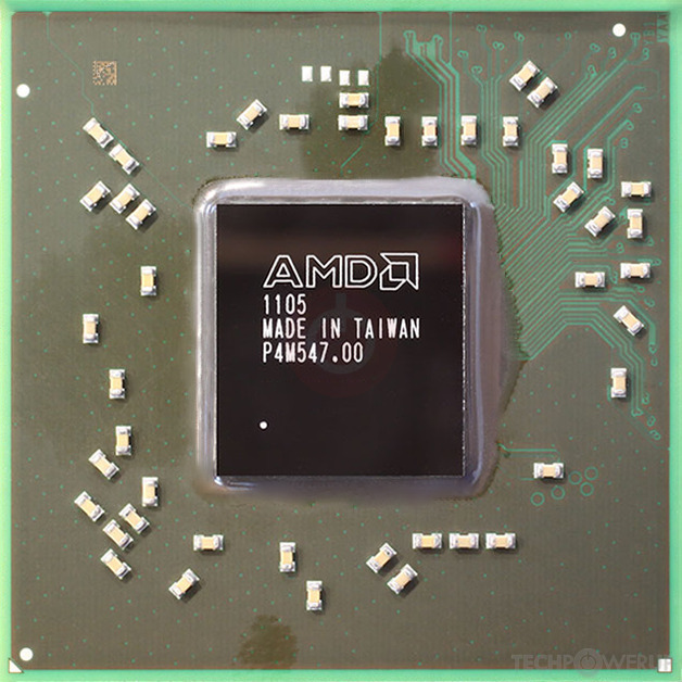
- Graphics Processor
- Thames
- Cores
- 480
- TMUs
- 24
- ROPs
- 16
- Memory Size
- 2 GB
- Memory Type
- DDR3
- Bus Width
- 128 bit

GPU
Graphics Processor
- GPU Name
- Thames
- GPU Variant
-
Thames M2 XT
(216-0833000)
- Architecture
- TeraScale 2
- Foundry
- TSMC
- Process Size
- 40 nm
- Transistors
- 716 million
- Density
- 6.1M / mm²
- Die Size
- 118 mm²
- Chip Package
- FCBGA-631/962
Mobile Graphics
- Release Date
- Feb 17th, 2012
- Generation
-
London
(HD 7600M)
- Predecessor
- Vancouver
- Successor
- Solar System
- Production
- End-of-life
- Bus Interface
- PCIe 2.0 x16
Clock Speeds
- GPU Clock
- 600 MHz
- Memory Clock
-
900 MHz
1800 Mbps effective
Memory
- Memory Size
-
1024 MB
2 GB
- Memory Type
- DDR3
- Memory Bus
- 128 bit
- Bandwidth
- 28.80 GB/s
Render Config
- Shading Units
- 480
- TMUs
- 24
- ROPs
- 16
- Compute Units
- 6
- L1 Cache
- 8 KB (per CU)
- L2 Cache
- 256 KB
Theoretical Performance
- Pixel Rate
- 9.600 GPixel/s
- Texture Rate
- 14.40 GTexel/s
- FP32 (float)
- 576.0 GFLOPS
Board Design
- TDP
- 20 W
- Outputs
- Portable Device Dependent
Graphics Features
- DirectX
- 11.2 (11_0)
- OpenGL
- 4.4
- OpenCL
- 1.2
- Vulkan
- N/A
- Shader Model
- 5.0
Card Notes
| Memory Variant: 1024MB GDDR3 Memory Variant: 2048MB GDDR3 |
Thames GPU Notes
| Generation: Northern Islands Desktop Variant: Turks Mobile Variant: Whistler Graphics/Compute: GFX4 Display Core Engine: 5.0 Unified Video Decoder: 3.1 |
Other retail boards based on this design (4)
| Name | GPU Clock | Memory Clock | Other Changes |
|---|---|---|---|
| 600 MHz | 900 MHz | GDDR5 | |
| 600 MHz | 900 MHz | 2 GB | |
|
HP HD 7670M 2 GB

|
600 MHz | 900 MHz | 2 GB |
| 600 MHz | 900 MHz | 2 GB |


Apr 16th, 2024 10:35 EDT
change timezone
Latest GPU Drivers
New Forum Posts
- Using a cable from 1 psu in another PC (9)
- Shadow Of The Tomb Raider - CPU Performance and general game benchmark discussions (523)
- DTS:X APO4 + DTS Interactive for Most Devices [USB Supported] (303)
- Which air cooler for a ryzen 9 5900x (148)
- Forza Motorsport discussion thread (167)
- Dell Workstation Owners Club (3047)
- [Win11] Double ¨¨ whenever I press the quotation key EVEN if English UK keyboard is not installed/active... How do I fix this? (1)
- Undervolting Dell XPS 14 9440 is it possible? (6)
- Cyberpunk 2077 Game Discussion (2116)
- Vega owners club (566)
Popular Reviews
- Horizon Forbidden West Performance Benchmark Review - 30 GPUs Tested
- PowerColor Radeon RX 7900 GRE Hellhound Review
- Galax GeForce RTX 4070 Super EX Review
- Fractal Design Terra Review
- ASUS GeForce RTX 4090 Matrix Platinum Review - The RTX 4090 Ti
- Corsair 2000D Airflow Review
- Minisforum EliteMini UM780 XTX (AMD Ryzen 7 7840HS) Review
- Creative Pebble X Plus Review
- FiiO KB3 HiFi Mechanical Keyboard Review - Integrated DAC/Amp!
- ASUS GeForce RTX 4090 STRIX OC Review
Controversial News Posts
- NVIDIA Points Intel Raptor Lake CPU Users to Get Help from Intel Amid System Instability Issues (102)
- US Government Wants Nuclear Plants to Offload AI Data Center Expansion (98)
- Sony PlayStation 5 Pro Specifications Confirmed, Console Arrives Before Holidays (91)
- Developers of Outpost Infinity Siege Recommend Underclocking i9-13900K and i9-14900K for Stability on Machines with RTX 4090 (82)
- Windows 10 Security Updates to Cost $61 After 2025, $427 by 2028 (79)
- TechPowerUp Hiring: Reviewers Wanted for Motherboards, Laptops, Gaming Handhelds and Prebuilt Desktops (70)
- Intel Realizes the Only Way to Save x86 is to Democratize it, Reopens x86 IP Licensing (70)
- AMD Zen 5 Execution Engine Leaked, Features True 512-bit FPU (63)