Report an Error


Inno3D P102-100 Twin X2
- MN102P-2SDN-P6D
- Graphics Processor
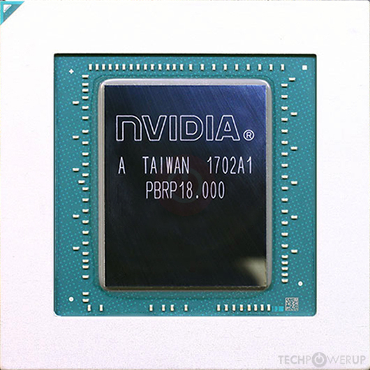
- GP102
- Cores
- 3200
- TMUs
- 200
- ROPs
- 80
- Memory Size
- 5 GB
- Memory Type
- GDDR5X
- Bus Width
- 320 bit

GPU
Graphics Processor
Graphics Card
Clock Speeds
- Base Clock
- 1582 MHz
- Boost Clock
- 1683 MHz
- Memory Clock
-
1376 MHz
11 Gbps effective
Memory
- Memory Size
- 5 GB
- Memory Type
- GDDR5X
- Memory Bus
- 320 bit
- Bandwidth
- 440.3 GB/s
Render Config
- Shading Units
- 3200
- TMUs
- 200
- ROPs
- 80
- SM Count
- 25
- L1 Cache
- 48 KB (per SM)
- L2 Cache
- 2.5 MB
Theoretical Performance
- Pixel Rate
- 134.6 GPixel/s
- Texture Rate
- 336.6 GTexel/s
- FP16 (half)
- 168.3 GFLOPS (1:64)
- FP32 (float)
- 10.77 TFLOPS
- FP64 (double)
- 336.6 GFLOPS (1:32)
Board Design
- Slot Width
- Dual-slot
- Length
267 mm
215 mm
10.5 inches
8.5 inches
- TDP
- 250 W
- Suggested PSU
- 600 W
- Outputs
- No outputs
- Power Connectors
- 2x 8-pin
- Board Number
- PG611 SKU 100
Graphics Features
- DirectX
- 12 (12_1)
- OpenGL
- 4.6
- OpenCL
- 3.0
- Vulkan
- 1.3
- CUDA
- 6.1
- Shader Model
- 6.7
GP102 GPU Notes
| NVENC: 6th Gen NVDEC: 3rd Gen PureVideo HD: VP8 VDPAU: Feature Set H |
Other retail boards based on this design (2)
| Name | GPU Clock | Boost Clock | Memory Clock | Other Changes |
|---|---|---|---|---|
|
Inno3D P102-100 Twin X2

|
1582 MHz | 1683 MHz | 1376 MHz | 215 mm/8.5 inches |
| 1582 MHz | 1683 MHz | 1376 MHz | 215 mm/8.5 inches |

Apr 16th, 2024 09:02 EDT
change timezone
Latest GPU Drivers
New Forum Posts
- Which air cooler for a ryzen 9 5900x (142)
- heatware is not getting enough people selling their hardwares (0)
- Forza Motorsport discussion thread (166)
- Vega owners club (566)
- FINAL FANTASY XIV: Dawntrail Official Benchmark (32)
- Visually does this GPU seem to have any problems? (10)
- USB C to USB A hub (41)
- Beware: Win11 KB5035853 Cumulative Update may cause stuttering and other performance problems. (15)
- Using a cable from 1 psu in another PC (2)
- Outer Worlds getting boring (13)
Popular Reviews
- Horizon Forbidden West Performance Benchmark Review - 30 GPUs Tested
- PowerColor Radeon RX 7900 GRE Hellhound Review
- Galax GeForce RTX 4070 Super EX Review
- Fractal Design Terra Review
- ASUS GeForce RTX 4090 Matrix Platinum Review - The RTX 4090 Ti
- Corsair 2000D Airflow Review
- Minisforum EliteMini UM780 XTX (AMD Ryzen 7 7840HS) Review
- Creative Pebble X Plus Review
- FiiO KB3 HiFi Mechanical Keyboard Review - Integrated DAC/Amp!
- ASUS GeForce RTX 4090 STRIX OC Review
Controversial News Posts
- NVIDIA Points Intel Raptor Lake CPU Users to Get Help from Intel Amid System Instability Issues (102)
- US Government Wants Nuclear Plants to Offload AI Data Center Expansion (98)
- Sony PlayStation 5 Pro Specifications Confirmed, Console Arrives Before Holidays (90)
- Developers of Outpost Infinity Siege Recommend Underclocking i9-13900K and i9-14900K for Stability on Machines with RTX 4090 (82)
- Windows 10 Security Updates to Cost $61 After 2025, $427 by 2028 (79)
- TechPowerUp Hiring: Reviewers Wanted for Motherboards, Laptops, Gaming Handhelds and Prebuilt Desktops (70)
- Intel Realizes the Only Way to Save x86 is to Democratize it, Reopens x86 IP Licensing (70)
- AMD Zen 5 Execution Engine Leaked, Features True 512-bit FPU (63)