Report an Error


NVIDIA G73

G73
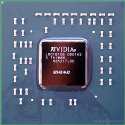
G73-GT-N-A2

G73M-U-N-A2

G73 BGA

SIC66SIC66
Die Shot
NVIDIA's G73 GPU uses the Curie architecture and is made using a 90 nm production process at TSMC. With a die size of 125 mm² and a transistor count of 177 million it is a small chip. G73 supports DirectX 9.0c (Feature Level 9_3). For GPU compute applications, OpenCL version N/A can be used. It features 12 pixel shaders and 5 vertex shaders, 12 texture mapping units and 8 ROPs. Due to the lack of unified shaders you will not be able to run recent games at all (which require unified shader/DX10+ support).
Graphics Processor
- Released
- Mar 1st, 2006
- GPU Name
- G73
- Codename
- NV4B
- Architecture
- Curie
- Foundry
- TSMC
- Process Size
- 90 nm
- Transistors
- 177 million
- Density
- 1.4M / mm²
- Die Size
- 125 mm²
- Package
- BGA-820
Graphics Features
- DirectX
- 9.0c (9_3)
- OpenGL
- 2.1
- OpenCL
- N/A
- Vulkan
- N/A
- Shader Model
- 3.0
- WDDM
- 1.0
- PureVideo HD
- VP1
- VDPAU
- No Support
Render Config
- Pixel Shaders
- 12
- Vertex Shaders
- 5
- TMUs
- 12
- ROPs
- 8
- Max. TDP
- 40 W
- Tex L1 Cache
- 16 KB per 4 PS
- Tex L2 Cache
- 32 KB per 4 PS
All Curie GPUs
NVIDIA GPU Architecture History
- 2023 Hopper
- 2022-2024 Ada Lovelace
- 2020-2024 Ampere
- 2018-2022 Turing
- 2017-2020 Volta
- 2016-2021 Pascal
- 2014-2019 Maxwell 2.0
- 2014-2017 Maxwell
- 2013-2015 Kepler 2.0
- 2012-2018 Kepler
- 2010-2016 Fermi 2.0
- 2010-2013 VLIW Vec4
- 2010-2016 Fermi
- 2007-2013 Tesla 2.0
- 2006-2010 Tesla
- 2003-2013 Curie
- 2003-2005 Rankine
- 2001-2003 Kelvin
- 1999-2005 Celsius
- 1998-2000 Fahrenheit
Graphics cards using the NVIDIA G73 GPU
| Name | Chip | Memory | Shaders | TMUs | ROPs | GPU Clock | Memory Clock |
|---|---|---|---|---|---|---|---|
| 128 MB | 12 / 5 | 12 | 8 | 350 MHz | 600 MHz | ||
| QD-NVS-300M-N-A2 | 256 MB | 8 / 4 | 8 | 8 | 500 MHz | 700 MHz | |
| GF-GO7600-N-A2 | 256 MB | 8 / 4 | 8 | 8 | 450 MHz | 350 MHz | |
| 128 MB | 12 / 5 | 12 | 8 | 450 MHz | 500 MHz | ||
| 256 MB | 12 / 5 | 12 | 8 | 350 MHz | 333 MHz | ||
| G73-GT-N-A2 | 128 MB | 8 / 4 | 8 | 8 | 350 MHz | 500 MHz | |
| G73-GT-N-A2 | 256 MB | 12 / 5 | 12 | 8 | 560 MHz | 700 MHz | |
| 128 MB | 8 / 4 | 8 | 8 | 350 MHz | 325 MHz |


G73 GPU Notes
| PureVideo HD: VP1 VDPAU: No Support |
Apr 17th, 2024 05:06 EDT
change timezone
Latest GPU Drivers
New Forum Posts
- AI Benchmark Alpha version 0.1.2 (1)
- Easy mistake - Easy fix (8)
- Your PC ATM (34469)
- Realtek INTELAUDIO (Dolby Home Theater v4 + Sonic Focus) for Windows 10 ≥1803 (10)
- What's your latest tech purchase? (20238)
- Nvidia Surround (1)
- Is there a technical reason that Windows 11 doesn't have built into it battery charge limitation? (22)
- Outer Worlds getting boring (29)
- Free Games Thread (3756)
- NVCleanInstall Error: Access to the path ”DisplayDriverExt.dll” is denied. (9)
Popular Reviews
- Horizon Forbidden West Performance Benchmark Review - 30 GPUs Tested
- PowerColor Radeon RX 7900 GRE Hellhound Review
- Fractal Design Terra Review
- ASUS GeForce RTX 4090 Matrix Platinum Review - The RTX 4090 Ti
- Corsair 2000D Airflow Review
- Minisforum EliteMini UM780 XTX (AMD Ryzen 7 7840HS) Review
- Creative Pebble X Plus Review
- FiiO KB3 HiFi Mechanical Keyboard Review - Integrated DAC/Amp!
- ASUS GeForce RTX 4090 STRIX OC Review
- NVIDIA GeForce RTX 4090 Founders Edition Review - Impressive Performance
Controversial News Posts
- Sony PlayStation 5 Pro Specifications Confirmed, Console Arrives Before Holidays (103)
- NVIDIA Points Intel Raptor Lake CPU Users to Get Help from Intel Amid System Instability Issues (102)
- US Government Wants Nuclear Plants to Offload AI Data Center Expansion (98)
- Developers of Outpost Infinity Siege Recommend Underclocking i9-13900K and i9-14900K for Stability on Machines with RTX 4090 (82)
- Windows 10 Security Updates to Cost $61 After 2025, $427 by 2028 (81)
- TechPowerUp Hiring: Reviewers Wanted for Motherboards, Laptops, Gaming Handhelds and Prebuilt Desktops (70)
- Intel Realizes the Only Way to Save x86 is to Democratize it, Reopens x86 IP Licensing (70)
- AMD Zen 5 Execution Engine Leaked, Features True 512-bit FPU (63)