Report an Error


NVIDIA G94

G94

G94-300-A1

G94 BGA
Oleg Kashirin
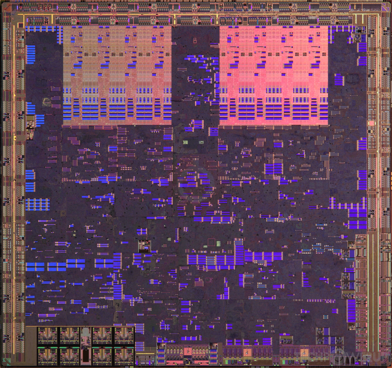
Die Shot

TPC Diagram
NVIDIA's G94 GPU uses the Tesla architecture and is made using a 65 nm production process at TSMC. With a die size of 240 mm² and a transistor count of 505 million it is a medium-sized chip. G94 supports DirectX 11.1 (Feature Level 10_0). For GPU compute applications, OpenCL version 1.1 and CUDA 1.1 can be used. It features 64 shading units, 32 texture mapping units and 16 ROPs.
Further reading:
Tesla Architecture Whitepaper 
Graphics Processor
- Released
- Feb 21st, 2008
- GPU Name
- G94
- Codename
- NV94
- Architecture
- Tesla
- Foundry
- TSMC
- Process Size
- 65 nm
- Transistors
- 505 million
- Density
- 2.1M / mm²
- Die Size
- 240 mm²
- Package
- BGA-1504
Graphics Features
- DirectX
- 11.1 (10_0)
- OpenGL
- 3.3
- OpenCL
- 1.1
- Vulkan
- N/A
- CUDA
- 1.1
- Shader Model
- 4.0
- WDDM
- 1.2
- PureVideo HD
- VP2
- VDPAU
- Feature Set A
Render Config
- Shading Units
- 64
- TMUs
- 32
- ROPs
- 16
- SM Count
- 8
- SFUs
- 16
- TPCs
- 4
- Tex L1 Cache
- 16 KB per TPC
- L2 Cache
- 64 KB
- Max. TDP
- 95 W
All Tesla GPUs
NVIDIA GPU Architecture History
- 2023 Hopper
- 2022-2024 Ada Lovelace
- 2020-2024 Ampere
- 2018-2022 Turing
- 2017-2020 Volta
- 2016-2021 Pascal
- 2014-2019 Maxwell 2.0
- 2014-2017 Maxwell
- 2013-2015 Kepler 2.0
- 2012-2018 Kepler
- 2010-2016 Fermi 2.0
- 2010-2013 VLIW Vec4
- 2010-2016 Fermi
- 2007-2013 Tesla 2.0
- 2006-2010 Tesla
- 2003-2013 Curie
- 2003-2005 Rankine
- 2001-2003 Kelvin
- 1999-2005 Celsius
- 1998-2000 Fahrenheit
Graphics cards using the NVIDIA G94 GPU
| Name | Chip | Memory | Shaders | TMUs | ROPs | GPU Clock | Memory Clock |
|---|---|---|---|---|---|---|---|
| G94-300-A1 | 512 MB | 64 | 32 | 16 | 650 MHz | 900 MHz | |
| G94-300-A1 | 512 MB | 48 | 24 | 16 | 650 MHz | 900 MHz | |
| G94-300-A1 | 768 MB | 48 | 24 | 12 | 500 MHz | 1000 MHz | |
| G94 GL-U | 768 MB | 64 | 32 | 12 | 550 MHz | 800 MHz | |
| NB9E-GLM2 | 512 MB | 48 | 24 | 16 | 530 MHz | 799 MHz | |
| N10E-GE1 | 1024 MB | 64 | 32 | 16 | 400 MHz | 800 MHz | |
| N10E-GS1 | 1024 MB | 64 | 32 | 16 | 600 MHz | 800 MHz | |
| NB9E-GT | 512 MB | 64 | 32 | 16 | 600 MHz | 800 MHz | |
| NB9E-GS1 | 512 MB | 64 | 32 | 16 | 530 MHz | 800 MHz | |
| NB9E-GS | 512 MB | 48 | 24 | 16 | 530 MHz | 800 MHz | |
| 9800S | 512 MB | 64 | 32 | 16 | 600 MHz | 799 MHz | |
| G94-300-A1 | 1024 MB | 64 | 32 | 16 | 600 MHz | 266 MHz | |
| 1024 MB | 48 | 24 | 8 | 600 MHz | 700 MHz | ||
| NB9E-GT1 | 1024 MB | 64 | 32 | 16 | 600 MHz | 800 MHz | |
| G94-300-A1 | 512 MB | 64 | 32 | 16 | 600 MHz | 700 MHz |


G94 GPU Notes
| PureVideo HD: VP2 VDPAU: Feature Set A |
Apr 24th, 2024 10:06 EDT
change timezone
Latest GPU Drivers
New Forum Posts
- Large Address Aware (374)
- Looking to build another system (3)
- ThrottleStop 9.6 Voltage won't change (3)
- EK seems to be having major issues (39)
- What's your latest tech purchase? (20334)
- Official Board Game Discussion (16)
- What phone you use as your daily driver? And, a discussion of them. (1464)
- My computer setup - Request for opinions (15)
- Is It The 1080 TI The Best GPU Ever? (205)
- Core i5-6300U (10)
Popular Reviews
- Fractal Design Terra Review
- Corsair 2000D Airflow Review
- Thermalright Phantom Spirit 120 EVO Review
- Minisforum EliteMini UM780 XTX (AMD Ryzen 7 7840HS) Review
- ASUS GeForce RTX 4090 STRIX OC Review
- NVIDIA GeForce RTX 4090 Founders Edition Review - Impressive Performance
- ASUS GeForce RTX 4090 Matrix Platinum Review - The RTX 4090 Ti
- MSI GeForce RTX 4090 Gaming X Trio Review
- MSI GeForce RTX 4090 Suprim X Review
- Gigabyte GeForce RTX 4090 Gaming OC Review
Controversial News Posts
- Sony PlayStation 5 Pro Specifications Confirmed, Console Arrives Before Holidays (116)
- NVIDIA Points Intel Raptor Lake CPU Users to Get Help from Intel Amid System Instability Issues (106)
- AMD "Strix Halo" Zen 5 Mobile Processor Pictured: Chiplet-based, Uses 256-bit LPDDR5X (101)
- US Government Wants Nuclear Plants to Offload AI Data Center Expansion (98)
- Windows 10 Security Updates to Cost $61 After 2025, $427 by 2028 (84)
- Developers of Outpost Infinity Siege Recommend Underclocking i9-13900K and i9-14900K for Stability on Machines with RTX 4090 (84)
- TechPowerUp Hiring: Reviewers Wanted for Motherboards, Laptops, Gaming Handhelds and Prebuilt Desktops (78)
- Intel Realizes the Only Way to Save x86 is to Democratize it, Reopens x86 IP Licensing (70)