Report an Error


NVIDIA GM206

GM206

GM206-250-A1
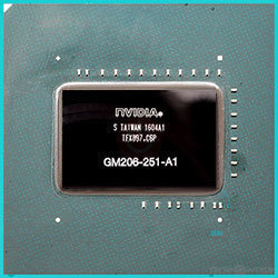
GM206-251-A1

GM206-300-A1

Block Diagram
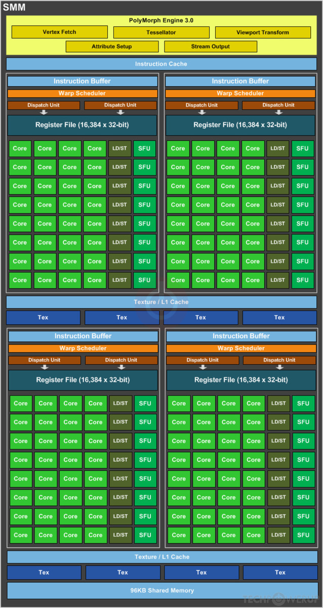
SMM Diagram
NVIDIA's GM206 GPU uses the Maxwell 2.0 architecture and is made using a 28 nm production process at TSMC. With a die size of 228 mm² and a transistor count of 2,940 million it is a medium-sized chip. GM206 supports DirectX 12 (Feature Level 12_1). For GPU compute applications, OpenCL version 3.0 and CUDA 5.2 can be used. It features 1024 shading units, 64 texture mapping units and 32 ROPs.
Graphics Processor
- Released
- Jan 22nd, 2015
- GPU Name
- GM206
- Codename
- NV126
- Architecture
- Maxwell 2.0
- Foundry
- TSMC
- Process Size
- 28 nm
- Transistors
- 2,940 million
- Density
- 12.9M / mm²
- Die Size
- 228 mm²
- Package
- BGA-1428
Graphics Features
- DirectX
- 12 (12_1)
- OpenGL
- 4.6
- OpenCL
- 3.0
- Vulkan
- 1.3
- CUDA
- 5.2
- Shader Model
- 6.7
- WDDM
- 3.1
- NVENC
- 5th Gen
- NVDEC
- 2nd Gen
- PureVideo HD
- VP7
- VDPAU
- Feature Set F
Render Config
- Shading Units
- 1024
- TMUs
- 64
- ROPs
- 32
- SMM Count
- 8
- GPCs
- 2
- L1 Cache
- 48 KB per SMM
- L2 Cache
- 1024 KB
- Max. TDP
- 120 W
- SFUs
- 256
All Maxwell 2.0 GPUs
- NVIDIA GM200
- NVIDIA GM204
- NVIDIA GM206
- NVIDIA GM206S
- NVIDIA GM20B
- NVIDIA GM20B
NVIDIA GPU Architecture History
- 2023 Hopper
- 2022-2024 Ada Lovelace
- 2020-2024 Ampere
- 2018-2022 Turing
- 2017-2020 Volta
- 2016-2021 Pascal
- 2014-2019 Maxwell 2.0
- 2014-2017 Maxwell
- 2013-2015 Kepler 2.0
- 2012-2018 Kepler
- 2010-2016 Fermi 2.0
- 2010-2013 VLIW Vec4
- 2010-2016 Fermi
- 2007-2013 Tesla 2.0
- 2006-2010 Tesla
- 2003-2013 Curie
- 2003-2005 Rankine
- 2001-2003 Kelvin
- 1999-2005 Celsius
- 1998-2000 Fahrenheit
Graphics cards using the NVIDIA GM206 GPU
| Name | Chip | Memory | Shaders | TMUs | ROPs | Base Clock | Boost Clock | Memory Clock |
|---|---|---|---|---|---|---|---|---|
| GM206-300-A1 | 2 GB | 1024 | 64 | 32 | 1127 MHz | 1178 MHz | 1753 MHz | |
| GM206-250-A1 | 2 GB | 768 | 48 | 32 | 1024 MHz | 1188 MHz | 1653 MHz | |
| 4 GB | 1024 | 64 | 32 | 872 MHz | 1072 MHz | 1375 MHz | ||
| 2 GB | 512 | 32 | 32 | 1087 MHz | 1239 MHz | 1253 MHz | ||
| GTX 960 OEM | 4 GB | 1024 | 64 | 32 | 1176 MHz | 1201 MHz | 1753 MHz | |
| GM206-875-A1 | 4 GB | 768 | 48 | 32 | 796 MHz | 1163 MHz | 1653 MHz | |
| GM206-251-A1 | 2 GB | 768 | 48 | 32 | 1026 MHz | 1190 MHz | 1653 MHz | |
| 4 GB | 1024 | 64 | 32 | 695 MHz | 1036 MHz | 1377 MHz |


GM206 GPU Notes
| NVENC: 5th Gen NVDEC: 2nd Gen PureVideo HD: VP7 VDPAU: Feature Set F |
Apr 20th, 2024 00:37 EDT
change timezone
Latest GPU Drivers
New Forum Posts
- Windows 11 General Discussion (5015)
- Roccat Kone AIMO has developed a double left click, when I click it once. Any fix out there? (39)
- Which air cooler for a ryzen 9 5900x (161)
- Liquidextasy waterblocks (51)
- I just succesfully baked DDR4 (76)
- GPU-Z reporting wrong ReBar info for RTX 20 series (4)
- I9 13890HX undervolting Suggestions (5)
- Official Board Game Discussion (4)
- Cinebench crashed my PC. My Wi-Fi stopped working, and I keep getting a "Please wait" screen when I boot up my PC. (8)
- USB C to USB A hub (43)
Popular Reviews
- Horizon Forbidden West Performance Benchmark Review - 30 GPUs Tested
- Fractal Design Terra Review
- Corsair 2000D Airflow Review
- Thermalright Phantom Spirit 120 EVO Review
- Minisforum EliteMini UM780 XTX (AMD Ryzen 7 7840HS) Review
- Creative Pebble X Plus Review
- FiiO KB3 HiFi Mechanical Keyboard Review - Integrated DAC/Amp!
- ASUS GeForce RTX 4090 STRIX OC Review
- NVIDIA GeForce RTX 4090 Founders Edition Review - Impressive Performance
- ASUS GeForce RTX 4090 Matrix Platinum Review - The RTX 4090 Ti
Controversial News Posts
- Sony PlayStation 5 Pro Specifications Confirmed, Console Arrives Before Holidays (111)
- NVIDIA Points Intel Raptor Lake CPU Users to Get Help from Intel Amid System Instability Issues (102)
- US Government Wants Nuclear Plants to Offload AI Data Center Expansion (98)
- AMD "Strix Halo" Zen 5 Mobile Processor Pictured: Chiplet-based, Uses 256-bit LPDDR5X (84)
- Windows 10 Security Updates to Cost $61 After 2025, $427 by 2028 (82)
- Developers of Outpost Infinity Siege Recommend Underclocking i9-13900K and i9-14900K for Stability on Machines with RTX 4090 (82)
- TechPowerUp Hiring: Reviewers Wanted for Motherboards, Laptops, Gaming Handhelds and Prebuilt Desktops (73)
- Intel Realizes the Only Way to Save x86 is to Democratize it, Reopens x86 IP Licensing (70)