Report an Error


NVIDIA GP100
GP100

GP100-890-A1

GP100-893-A1

GP100-897-A1

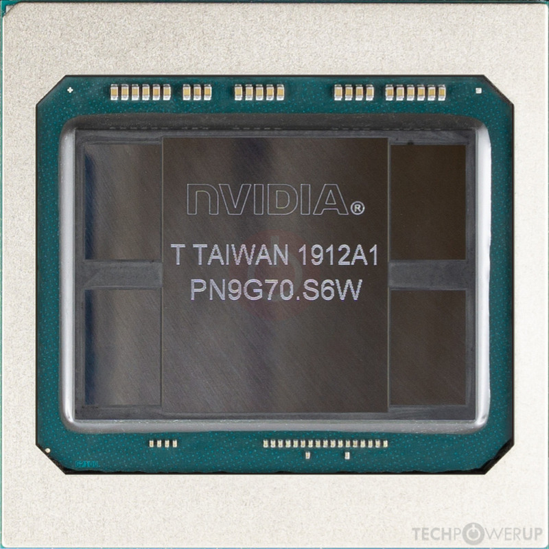
Die Shot

Block Diagram

SM Diagram
NVIDIA's GP100 GPU uses the Pascal architecture and is made using a 16 nm production process at TSMC. With a die size of 610 mm² and a transistor count of 15,300 million it is a very big chip. GP100 supports DirectX 12 (Feature Level 12_1). For GPU compute applications, OpenCL version 3.0 and CUDA 6.0 can be used. It features 3840 shading units, 240 texture mapping units and 96 ROPs.
Further reading:
GP100 Architecture Whitepaper 
Graphics Processor
- Released
- Apr 5th, 2016
- GPU Name
- GP100
- Codename
- NV130
- Architecture
- Pascal
- Foundry
- TSMC
- Process Size
- 16 nm
- Transistors
- 15,300 million
- Density
- 25.1M / mm²
- Die Size
- 610 mm²
- Package
- BGA-2621
Graphics Features
- DirectX
- 12 (12_1)
- OpenGL
- 4.6
- OpenCL
- 3.0
- Vulkan
- 1.3
- CUDA
- 6.0
- Shader Model
- 6.0
- WDDM
- 3.1
- NVENC
- 6th Gen
- NVDEC
- 3rd Gen
- PureVideo HD
- VP8
- VDPAU
- Feature Set H
Render Config
- Shading Units
- 3840
- TMUs
- 240
- ROPs
- 96
- SM Count
- 60
- SFUs
- 960
- TPCs
- 30
- GPCs
- 6
- L1 Cache
- 24 KB per SM
- L2 Cache
- 4096 KB
- Max. TDP
- 300 W
All Pascal GPUs
NVIDIA GPU Architecture History
- 2023 Hopper
- 2022-2024 Ada Lovelace
- 2020-2024 Ampere
- 2018-2022 Turing
- 2017-2020 Volta
- 2016-2021 Pascal
- 2014-2019 Maxwell 2.0
- 2014-2017 Maxwell
- 2013-2015 Kepler 2.0
- 2012-2018 Kepler
- 2010-2016 Fermi 2.0
- 2010-2013 VLIW Vec4
- 2010-2016 Fermi
- 2007-2013 Tesla 2.0
- 2006-2010 Tesla
- 2003-2013 Curie
- 2003-2005 Rankine
- 2001-2003 Kelvin
- 1999-2005 Celsius
- 1998-2000 Fahrenheit
Graphics cards using the NVIDIA GP100 GPU
| Name | Chip | Memory | Shaders | TMUs | ROPs | Base Clock | Boost Clock | Memory Clock |
|---|---|---|---|---|---|---|---|---|
| GP100-893-A1 | 16 GB | 3584 | 224 | 96 | 1190 MHz | 1329 MHz | 715 MHz | |
| GP100-892-A1 | 12 GB | 3584 | 224 | 96 | 1190 MHz | 1329 MHz | 715 MHz | |
| GP100-897-A1 | 16 GB | 3584 | 224 | 96 | 1304 MHz | 1443 MHz | 715 MHz | |
| GP100-890-A1 | 16 GB | 3584 | 224 | 96 | 1328 MHz | 1480 MHz | 715 MHz | |
| 16 GB | 3584 | 224 | 96 | 1328 MHz | 1480 MHz | 715 MHz |


GP100 GPU Notes
| NVENC: 6th Gen NVDEC: 3rd Gen PureVideo HD: VP8 VDPAU: Feature Set H |
Apr 23rd, 2024 20:41 EDT
change timezone
Latest GPU Drivers
New Forum Posts
- What's your latest tech purchase? (20319)
- Post your Cinebench 2024 score (449)
- Sexy Mechanical Keyboard Thread (484)
- The TPU UK Clubhouse (24766)
- need help with motherboard/ ram compability certainty (14)
- My computer setup - Request for opinions (12)
- Show us your collections thread!! (282)
- Realtek Modded Audio Driver for Windows 10/11 - Only for HDAUDIO (5687)
- What phone you use as your daily driver? And, a discussion of them. (1454)
- Is there a technical reason that Windows 11 doesn't have built into it battery charge limitation? (37)
Popular Reviews
- Fractal Design Terra Review
- Corsair 2000D Airflow Review
- Thermalright Phantom Spirit 120 EVO Review
- Minisforum EliteMini UM780 XTX (AMD Ryzen 7 7840HS) Review
- ASUS GeForce RTX 4090 STRIX OC Review
- NVIDIA GeForce RTX 4090 Founders Edition Review - Impressive Performance
- ASUS GeForce RTX 4090 Matrix Platinum Review - The RTX 4090 Ti
- MSI GeForce RTX 4090 Gaming X Trio Review
- MSI GeForce RTX 4090 Suprim X Review
- Gigabyte GeForce RTX 4090 Gaming OC Review
Controversial News Posts
- Sony PlayStation 5 Pro Specifications Confirmed, Console Arrives Before Holidays (116)
- NVIDIA Points Intel Raptor Lake CPU Users to Get Help from Intel Amid System Instability Issues (106)
- AMD "Strix Halo" Zen 5 Mobile Processor Pictured: Chiplet-based, Uses 256-bit LPDDR5X (101)
- US Government Wants Nuclear Plants to Offload AI Data Center Expansion (98)
- Windows 10 Security Updates to Cost $61 After 2025, $427 by 2028 (84)
- Developers of Outpost Infinity Siege Recommend Underclocking i9-13900K and i9-14900K for Stability on Machines with RTX 4090 (84)
- TechPowerUp Hiring: Reviewers Wanted for Motherboards, Laptops, Gaming Handhelds and Prebuilt Desktops (74)
- Intel Realizes the Only Way to Save x86 is to Democratize it, Reopens x86 IP Licensing (70)