Report an Error


NVIDIA GP107S

GP107S

GP107-670-A1

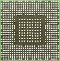
GP107S BGA

Block Diagram
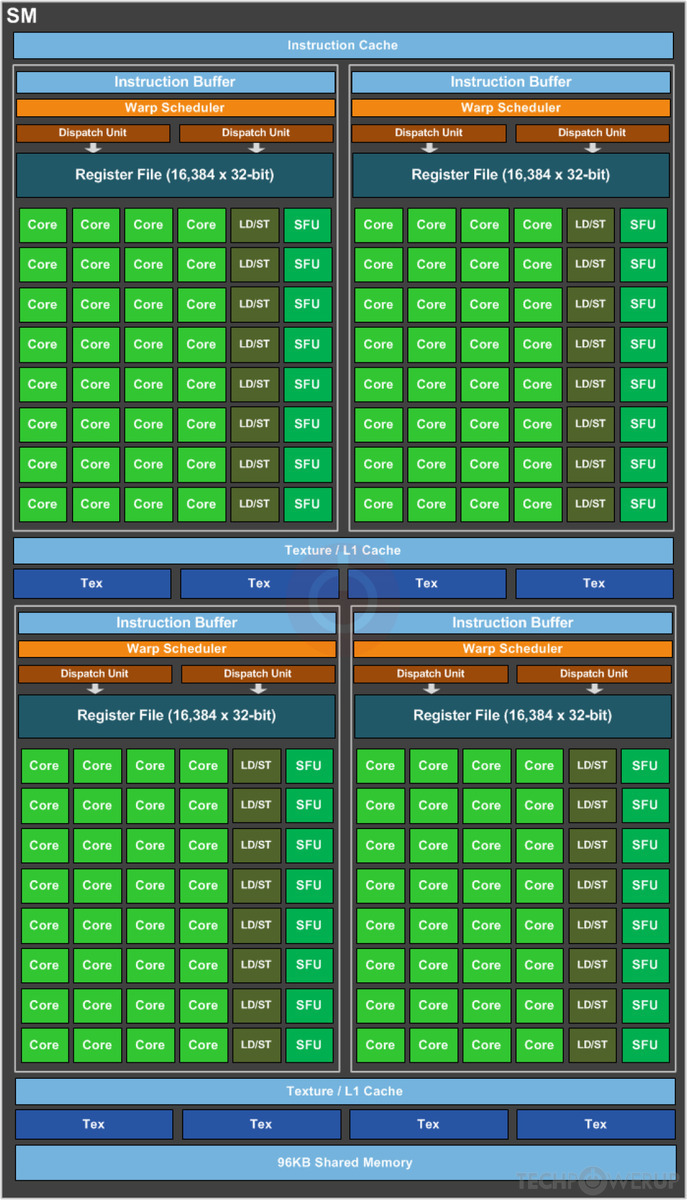
SM Diagram
NVIDIA's GP107S GPU uses the Pascal architecture and is made using a 14 nm production process at Samsung. With a die size of 132 mm² and a transistor count of 3,300 million it is a small chip. GP107S supports DirectX 12 (Feature Level 12_1). For GPU compute applications, OpenCL version 3.0 and CUDA 6.1 can be used. It features 640 shading units, 32 texture mapping units and 16 ROPs.
Graphics Processor
- Released
- Feb 10th, 2020
- GPU Name
- GP107S
- Codename
- NV137
- Architecture
- Pascal
- Foundry
- Samsung
- Process Size
- 14 nm
- Transistors
- 3,300 million
- Density
- 25.0M / mm²
- Die Size
- 132 mm²
- Package
- BGA-595
Graphics Features
- DirectX
- 12 (12_1)
- OpenGL
- 4.6
- OpenCL
- 3.0
- Vulkan
- 1.3
- CUDA
- 6.1
- Shader Model
- 6.7
- WDDM
- 3.1
- NVENC
- No Support
- NVDEC
- 3rd Gen
- PureVideo HD
- VP8
- VDPAU
- Feature Set H
Render Config
- Shading Units
- 640
- TMUs
- 32
- ROPs
- 16
- SM Count
- 5
- SFUs
- 192
- TPCs
- 6
- GPCs
- 2
- L1 Cache
- 48 KB per SM
- L2 Cache
- 512 KB
- Max. TDP
- 20 W
All Pascal GPUs
NVIDIA GPU Architecture History
- 2023 Hopper
- 2022-2024 Ada Lovelace
- 2020-2024 Ampere
- 2018-2022 Turing
- 2017-2020 Volta
- 2016-2021 Pascal
- 2014-2019 Maxwell 2.0
- 2014-2017 Maxwell
- 2013-2015 Kepler 2.0
- 2012-2018 Kepler
- 2010-2016 Fermi 2.0
- 2010-2013 VLIW Vec4
- 2010-2016 Fermi
- 2007-2013 Tesla 2.0
- 2006-2010 Tesla
- 2003-2013 Curie
- 2003-2005 Rankine
- 2001-2003 Kelvin
- 1999-2005 Celsius
- 1998-2000 Fahrenheit
Graphics cards using the NVIDIA GP107S GPU
| Name | Chip | Memory | Shaders | TMUs | ROPs | Base Clock | Boost Clock | Memory Clock |
|---|---|---|---|---|---|---|---|---|
| GP107-670-A1 | 2 GB | 640 | 32 | 16 | 1354 MHz | 1468 MHz | 1752 MHz | |
| GP107-670-A1 | 2 GB | 640 | 32 | 16 | 747 MHz | 937 MHz | 1752 MHz |
GP107S GPU Notes
| NVENC: No Support NVDEC: 3rd Gen PureVideo HD: VP8 VDPAU: Feature Set H |
Apr 23rd, 2024 10:03 EDT
change timezone
Latest GPU Drivers
New Forum Posts
- Windows 12 (142)
- Possible near-future 2024 Arrow Lake build.... (48)
- EK seems to be having major issues (25)
- Odd RTX 3080 behaviour (2)
- Show us your collections thread!! (281)
- Serious bug in PHP reported! (2)
- Upgrade Build (105)
- The Official Linux/Unix Desktop Screenshots Megathread (693)
- Share your AIDA 64 cache and memory benchmark here (2913)
- My computer setup - Request for opinions (4)
Popular Reviews
- Horizon Forbidden West Performance Benchmark Review - 30 GPUs Tested
- Fractal Design Terra Review
- Corsair 2000D Airflow Review
- Thermalright Phantom Spirit 120 EVO Review
- Minisforum EliteMini UM780 XTX (AMD Ryzen 7 7840HS) Review
- ASUS GeForce RTX 4090 STRIX OC Review
- NVIDIA GeForce RTX 4090 Founders Edition Review - Impressive Performance
- ASUS GeForce RTX 4090 Matrix Platinum Review - The RTX 4090 Ti
- Creative Pebble X Plus Review
- MSI GeForce RTX 4090 Gaming X Trio Review
Controversial News Posts
- Sony PlayStation 5 Pro Specifications Confirmed, Console Arrives Before Holidays (116)
- NVIDIA Points Intel Raptor Lake CPU Users to Get Help from Intel Amid System Instability Issues (105)
- AMD "Strix Halo" Zen 5 Mobile Processor Pictured: Chiplet-based, Uses 256-bit LPDDR5X (101)
- US Government Wants Nuclear Plants to Offload AI Data Center Expansion (98)
- Windows 10 Security Updates to Cost $61 After 2025, $427 by 2028 (84)
- Developers of Outpost Infinity Siege Recommend Underclocking i9-13900K and i9-14900K for Stability on Machines with RTX 4090 (82)
- TechPowerUp Hiring: Reviewers Wanted for Motherboards, Laptops, Gaming Handhelds and Prebuilt Desktops (74)
- Intel Realizes the Only Way to Save x86 is to Democratize it, Reopens x86 IP Licensing (70)