Report an Error


NVIDIA NV5

Vanta LT

Vanta
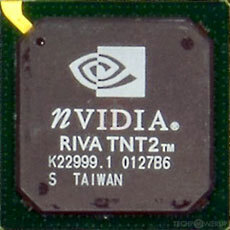
Riva TNT2

Riva TNT2 64

Vanta-16
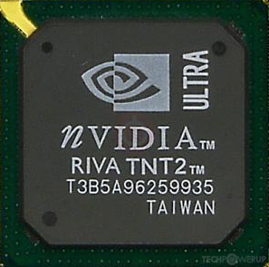
Riva TNT2 Ultra
Oleg Kashirin
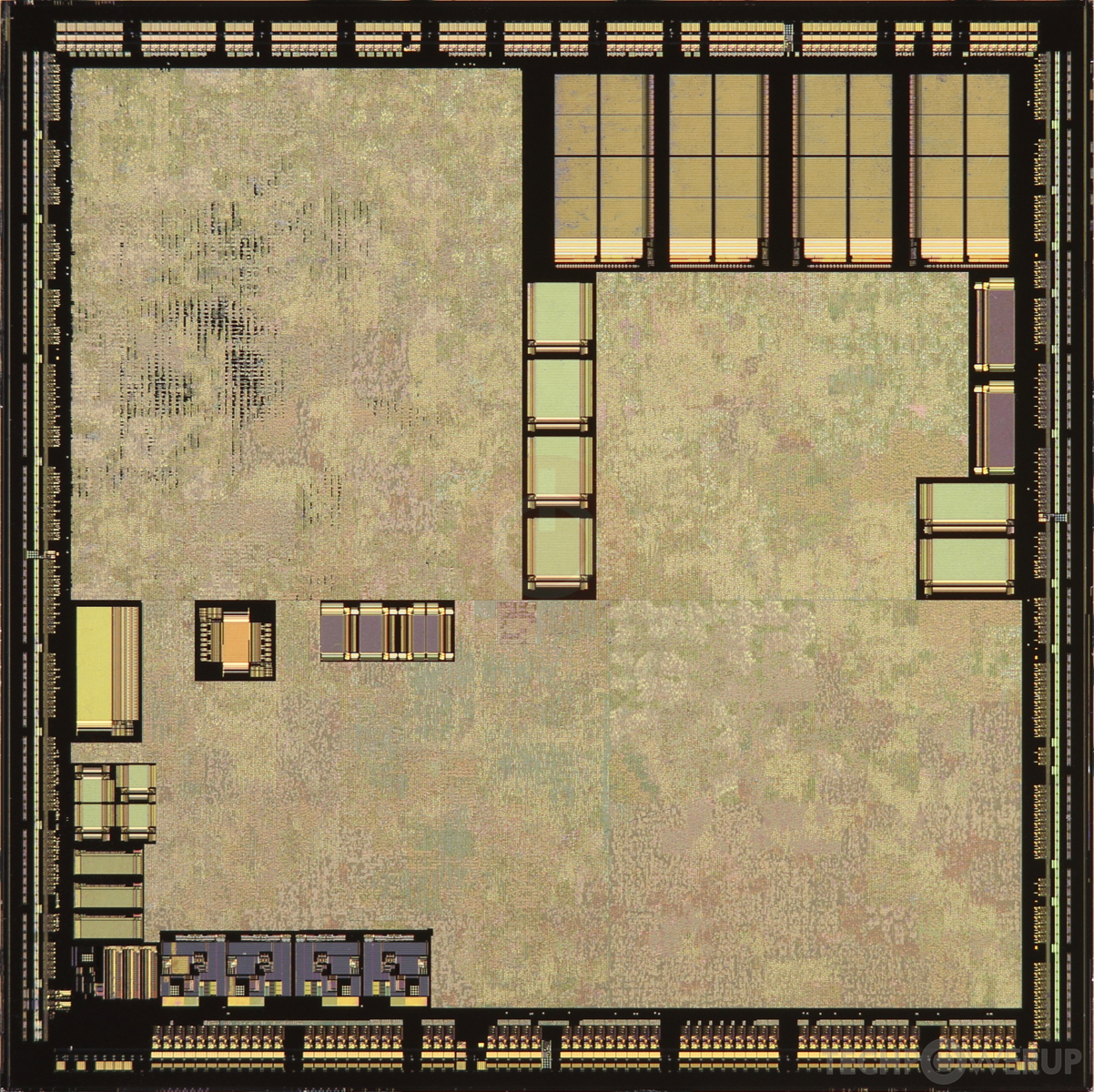
Die Shot
NVIDIA's NV5 GPU uses the Fahrenheit architecture and is made using a 250 nm production process at TSMC. With a die size of 63 mm² and a transistor count of 15 million it is a very small chip. NV5 supports DirectX 6.0. For GPU compute applications, OpenCL version N/A can be used. It features 2 pixel shaders and 0 vertex shaders, 2 texture mapping units and 2 ROPs. Due to the lack of unified shaders you will not be able to run recent games at all (which require unified shader/DX10+ support).
Graphics Processor
- Released
- Mar 15th, 1999
- GPU Name
- NV5
- Architecture
- Fahrenheit
- Foundry
- TSMC
- Process Size
- 250 nm
- Transistors
- 15 million
- Density
- 238.1K / mm²
- Die Size
- 63 mm²
Graphics Features
- DirectX
- 6.0
- OpenGL
- 1.2
- OpenCL
- N/A
- Vulkan
- N/A
- Pixel Shader
- N/A
- Vertex Shader
- N/A
Render Config
- Pixel Shaders
- 2
- Vertex Shaders
- 0
- TMUs
- 2
- ROPs
- 2
All Fahrenheit GPUs
- NVIDIA NV4
- NVIDIA NV5
NVIDIA GPU Architecture History
- 2023 Hopper
- 2022-2024 Ada Lovelace
- 2020-2024 Ampere
- 2018-2022 Turing
- 2017-2020 Volta
- 2016-2021 Pascal
- 2014-2019 Maxwell 2.0
- 2014-2017 Maxwell
- 2013-2015 Kepler 2.0
- 2012-2018 Kepler
- 2010-2016 Fermi 2.0
- 2010-2013 VLIW Vec4
- 2010-2016 Fermi
- 2007-2013 Tesla 2.0
- 2006-2010 Tesla
- 2003-2013 Curie
- 2003-2005 Rankine
- 2001-2003 Kelvin
- 1999-2005 Celsius
- 1998-2000 Fahrenheit
Graphics cards using the NVIDIA NV5 GPU
| Name | Chip | Memory | Shaders | TMUs | ROPs | GPU Clock | Memory Clock |
|---|---|---|---|---|---|---|---|
| Riva TNT2 Ultra | 32 MB | 2 / 0 | 2 | 2 | 150 MHz | 183 MHz | |
| Riva TNT2 | 32 MB | 2 / 0 | 2 | 2 | 143 MHz | 167 MHz | |
| Riva TNT2 | 16 MB | 2 / 0 | 2 | 2 | 125 MHz | 143 MHz | |
| Vanta-16 | 16 MB | 2 / 0 | 2 | 2 | 100 MHz | 133 MHz | |
| Vanta LT | 8 MB | 2 / 0 | 2 | 2 | 105 MHz | 100 MHz | |
| Vanta | 16 MB | 2 / 0 | 2 | 2 | 100 MHz | 133 MHz | |
| Riva TNT2 | 16 MB | 2 / 0 | 2 | 2 | 125 MHz | 150 MHz |


NV5 GPU Notes
| 2nd Generation 128-bit TwiN Texel architecture |
Apr 25th, 2024 02:53 EDT
change timezone
Latest GPU Drivers
New Forum Posts
- Core i5-6300U (13)
- GTX 1070 Ti - TDP Issues - Always Power Throttling (5)
- What phone you use as your daily driver? And, a discussion of them. (1471)
- Github comments used to push malware via Microsoft repo urls (2)
- The TPU UK Clubhouse (24784)
- (Anti) SFF fun house (349)
- What's your latest tech purchase? (20337)
- The Official Linux/Unix Desktop Screenshots Megathread (694)
- XFX RX470 8GB no video and error 43 (27)
- Cinebench crashed my PC. My Wi-Fi stopped working, and I keep getting a "Please wait" screen when I boot up my PC. (31)
Popular Reviews
- Fractal Design Terra Review
- Thermalright Phantom Spirit 120 EVO Review
- Corsair 2000D Airflow Review
- Minisforum EliteMini UM780 XTX (AMD Ryzen 7 7840HS) Review
- ASUS GeForce RTX 4090 STRIX OC Review
- NVIDIA GeForce RTX 4090 Founders Edition Review - Impressive Performance
- ASUS GeForce RTX 4090 Matrix Platinum Review - The RTX 4090 Ti
- MSI GeForce RTX 4090 Suprim X Review
- MSI GeForce RTX 4090 Gaming X Trio Review
- Gigabyte GeForce RTX 4090 Gaming OC Review
Controversial News Posts
- Sony PlayStation 5 Pro Specifications Confirmed, Console Arrives Before Holidays (116)
- NVIDIA Points Intel Raptor Lake CPU Users to Get Help from Intel Amid System Instability Issues (106)
- AMD "Strix Halo" Zen 5 Mobile Processor Pictured: Chiplet-based, Uses 256-bit LPDDR5X (101)
- US Government Wants Nuclear Plants to Offload AI Data Center Expansion (98)
- Windows 10 Security Updates to Cost $61 After 2025, $427 by 2028 (84)
- Developers of Outpost Infinity Siege Recommend Underclocking i9-13900K and i9-14900K for Stability on Machines with RTX 4090 (84)
- TechPowerUp Hiring: Reviewers Wanted for Motherboards, Laptops, Gaming Handhelds and Prebuilt Desktops (78)
- AMD's RDNA 4 GPUs Could Stick with 18 Gbps GDDR6 Memory (74)