Report an Error

NVIDIA PG506-232
- Graphics Processor
- GA100
- Cores
- 3584
- TMUs
- 224
- ROPs
- 96
- Memory Size
- 24 GB
- Memory Type
- HBM2
- Bus Width
- 3072 bit
GPU
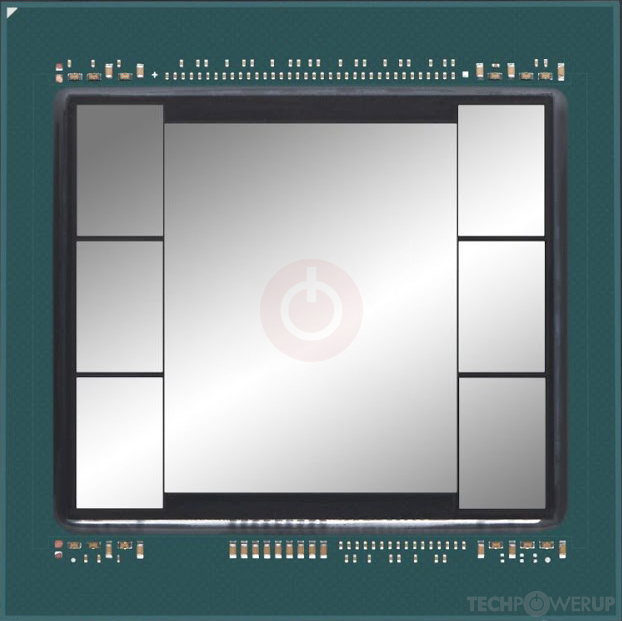
The PG506-232 is a professional graphics card by NVIDIA, launched on April 12th, 2021. Built on the 7 nm process, and based on the GA100 graphics processor, the card does not support DirectX. Since PG506-232 does not support DirectX 11 or DirectX 12, it might not be able to run all the latest games. The GA100 graphics processor is a large chip with a die area of 826 mm² and 54,200 million transistors. Unlike the fully unlocked DRIVE A100 PROD, which uses the same GPU but has all 6912 shaders enabled, NVIDIA has disabled some shading units on the PG506-232 to reach the product's target shader count. It features 3584 shading units, 224 texture mapping units, and 96 ROPs. Also included are 224 tensor cores which help improve the speed of machine learning applications. NVIDIA has paired 24 GB HBM2 memory with the PG506-232, which are connected using a 3072-bit memory interface. The GPU is operating at a frequency of 930 MHz, which can be boosted up to 1440 MHz, memory is running at 1215 MHz.
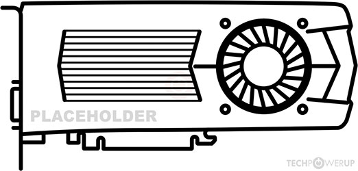
Being a dual-slot card, the NVIDIA PG506-232 draws power from an 8-pin EPS power connector, with power draw rated at 165 W maximum. This device has no display connectivity, as it is not designed to have monitors connected to it. PG506-232 is connected to the rest of the system using a PCI-Express 4.0 x16 interface. The card measures 267 mm in length, 112 mm in width, and features a dual-slot cooling solution.
Being a dual-slot card, the NVIDIA PG506-232 draws power from an 8-pin EPS power connector, with power draw rated at 165 W maximum. This device has no display connectivity, as it is not designed to have monitors connected to it. PG506-232 is connected to the rest of the system using a PCI-Express 4.0 x16 interface. The card measures 267 mm in length, 112 mm in width, and features a dual-slot cooling solution.
Graphics Processor
Graphics Card
- Release Date
- Apr 12th, 2021
- Availability
- 2021
- Generation
-
Tesla Ampere
(Axx)
- Predecessor
- Tesla Turing
- Successor
- Tesla Ada
- Production
- Active
- Bus Interface
- PCIe 4.0 x16
Relative Performance
Based on TPU review data: "Performance Summary" at 1920x1080, 4K for 2080 Ti and faster.
Performance estimated based on architecture, shader count and clocks.
Clock Speeds
- Base Clock
- 930 MHz
- Boost Clock
- 1440 MHz
- Memory Clock
-
1215 MHz
2.4 Gbps effective
Memory
- Memory Size
- 24 GB
- Memory Type
- HBM2
- Memory Bus
- 3072 bit
- Bandwidth
- 933.1 GB/s
Render Config
- Shading Units
- 3584
- TMUs
- 224
- ROPs
- 96
- SM Count
- 56
- Tensor Cores
- 224
- L1 Cache
- 192 KB (per SM)
- L2 Cache
- 24 MB
Theoretical Performance
- Pixel Rate
- 138.2 GPixel/s
- Texture Rate
- 322.6 GTexel/s
- FP16 (half)
- 10.32 TFLOPS (1:1)
- FP32 (float)
- 10.32 TFLOPS
- FP64 (double)
- 5.161 TFLOPS (1:2)
Board Design
- Slot Width
- Dual-slot
- Length
- 267 mm
10.5 inches
- Width
- 112 mm
4.4 inches
- TDP
- 165 W
- Suggested PSU
- 450 W
- Outputs
- No outputs
- Power Connectors
- 8-pin EPS
- Board Number
- P1001 SKU 205
Graphics Features
- DirectX
- N/A
- OpenGL
- N/A
- OpenCL
- 3.0
- Vulkan
- N/A
- CUDA
- 8.0
- Shader Model
- N/A
GA100 GPU Notes
| Tensor Cores: 3rd Gen NVENC: No Support NVDEC: 4th Gen x5 PureVideo HD: VP10 VDPAU: Feature Set J |
Apr 19th, 2024 22:51 EDT
change timezone
Latest GPU Drivers
New Forum Posts
- GPU-Z reporting wrong ReBar info for RTX 20 series (2)
- Official Board Game Discussion (4)
- I just succesfully baked DDR4 (73)
- Roccat Kone AIMO has developed a double left click, when I click it once. Any fix out there? (37)
- Cinebench crashed my PC. My Wi-Fi stopped working, and I keep getting a "Please wait" screen when I boot up my PC. (8)
- USB C to USB A hub (43)
- XFX RX580 stock Bios (8)
- Your PC ATM (34488)
- 2 questions about Oculus Quest 3 (0)
- Liquidextasy waterblocks (50)
Popular Reviews
- Horizon Forbidden West Performance Benchmark Review - 30 GPUs Tested
- Fractal Design Terra Review
- Corsair 2000D Airflow Review
- Thermalright Phantom Spirit 120 EVO Review
- Minisforum EliteMini UM780 XTX (AMD Ryzen 7 7840HS) Review
- Creative Pebble X Plus Review
- FiiO KB3 HiFi Mechanical Keyboard Review - Integrated DAC/Amp!
- ASUS GeForce RTX 4090 STRIX OC Review
- NVIDIA GeForce RTX 4090 Founders Edition Review - Impressive Performance
- ASUS GeForce RTX 4090 Matrix Platinum Review - The RTX 4090 Ti
Controversial News Posts
- Sony PlayStation 5 Pro Specifications Confirmed, Console Arrives Before Holidays (111)
- NVIDIA Points Intel Raptor Lake CPU Users to Get Help from Intel Amid System Instability Issues (102)
- US Government Wants Nuclear Plants to Offload AI Data Center Expansion (98)
- AMD "Strix Halo" Zen 5 Mobile Processor Pictured: Chiplet-based, Uses 256-bit LPDDR5X (84)
- Windows 10 Security Updates to Cost $61 After 2025, $427 by 2028 (82)
- Developers of Outpost Infinity Siege Recommend Underclocking i9-13900K and i9-14900K for Stability on Machines with RTX 4090 (82)
- TechPowerUp Hiring: Reviewers Wanted for Motherboards, Laptops, Gaming Handhelds and Prebuilt Desktops (72)
- Intel Realizes the Only Way to Save x86 is to Democratize it, Reopens x86 IP Licensing (70)