Report an Error


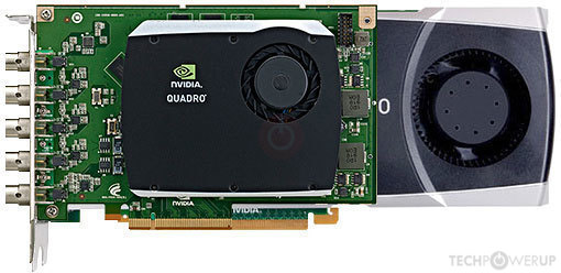
NVIDIA Quadro 5000 SDI
- Graphics Processor
- GF100
- Cores
- 352
- TMUs
- 44
- ROPs
- 40
- Memory Size
- 2.5 GB
- Memory Type
- GDDR5
- Bus Width
- 320 bit
GPU

I/O

Back
Recommended Gaming Resolutions:
- 1366x768
- 1600x900
- 1920x1080
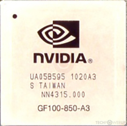
The Quadro 5000 SDI was an enthusiast-class professional graphics card by NVIDIA, launched on February 23rd, 2011. Built on the 40 nm process, and based on the GF100 graphics processor, in its GF100-850-A3 variant, the card supports DirectX 12. The GF100 graphics processor is a large chip with a die area of 529 mm² and 3,100 million transistors. Unlike the fully unlocked GeForce GTX 480 Core 512, which uses the same GPU but has all 512 shaders enabled, NVIDIA has disabled some shading units on the Quadro 5000 SDI to reach the product's target shader count. It features 352 shading units, 44 texture mapping units, and 40 ROPs. NVIDIA has paired 2,560 MB GDDR5 memory with the Quadro 5000 SDI, which are connected using a 320-bit memory interface. The GPU is operating at a frequency of 513 MHz, memory is running at 750 MHz (3 Gbps effective).
Being a quad-slot card, its power draw is rated at 172 W maximum. Display outputs include: 1x DVI, 2x DisplayPort, 1x S-Video, 2x SDI. Quadro 5000 SDI is connected to the rest of the system using a PCI-Express 2.0 x16 interface. The card measures 248 mm in length, 111 mm in width, and features a quad-slot cooling solution. Its price at launch was 7899 US Dollars.
Being a quad-slot card, its power draw is rated at 172 W maximum. Display outputs include: 1x DVI, 2x DisplayPort, 1x S-Video, 2x SDI. Quadro 5000 SDI is connected to the rest of the system using a PCI-Express 2.0 x16 interface. The card measures 248 mm in length, 111 mm in width, and features a quad-slot cooling solution. Its price at launch was 7899 US Dollars.
Graphics Processor
Graphics Card
- Release Date
- Feb 23rd, 2011
- Generation
-
Quadro Fermi
(x000)
- Predecessor
- Quadro FX Tesla
- Successor
- Quadro Kepler
- Production
- End-of-life
- Launch Price
- 7,899 USD
- Bus Interface
- PCIe 2.0 x16
- Reviews
- 26 in our database
Relative Performance
Based on TPU review data: "Performance Summary" at 1920x1080, 4K for 2080 Ti and faster.
Performance estimated based on architecture, shader count and clocks.
Clock Speeds
- GPU Clock
- 513 MHz
- Shader Clock
- 1026 MHz
- Memory Clock
-
750 MHz
3 Gbps effective
Memory
- Memory Size
- 2.5 GB
- Memory Type
- GDDR5
- Memory Bus
- 320 bit
- Bandwidth
- 120.0 GB/s
Render Config
- Shading Units
- 352
- TMUs
- 44
- ROPs
- 40
- SM Count
- 11
- L1 Cache
- 64 KB (per SM)
- L2 Cache
- 640 KB
Theoretical Performance
- Pixel Rate
- 11.29 GPixel/s
- Texture Rate
- 22.57 GTexel/s
- FP32 (float)
- 722.3 GFLOPS
- FP64 (double)
- 361.2 GFLOPS (1:2)
Board Design
- Slot Width
- Quad-slot
- Length
- 248 mm
9.8 inches
- Width
- 111 mm
4.4 inches
- TDP
- 172 W
- Suggested PSU
- 450 W
- Outputs
- 1x DVI
2x DisplayPort
1x S-Video
2x SDI
Graphics Features
- DirectX
- 12 (11_0)
- OpenGL
- 4.6
- OpenCL
- 1.1
- Vulkan
- N/A
- CUDA
- 2.0
- Shader Model
- 5.1
GF100 GPU Notes
| PureVideo HD: VP4 VDPAU: Feature Set C GF100 has 4 GPCs each capable of 8 pixels per clock. This limits complete GPU to 32 pixels per clock and because of that it can't feed all 48 ROPs when they all require data at the same time. Additional ROPs however can be used for MSAA (because it doesn't require additional data from rasterizers, while giving more work to ROPs.) |
Apr 25th, 2024 11:55 EDT
change timezone
Latest GPU Drivers
New Forum Posts
- Milestones (13874)
- WCG Daily Numbers (12496)
- TPU's Rosetta Milestones and Daily Pie Thread (1859)
- ThrottleStop 9.6 Voltage won't change (4)
- Folding Pie and Milestones!! (9008)
- Making Audio Enhancers Work on Windows (2649)
- Random blue screen from winload.efi error (0xc000000e) (1)
- which new soundcard or which 4.1 speakers kits ? (10)
- Alphacool CORE 1 CPU block - bulging with danger of splitting? (8)
- Free Games Thread (3767)
Popular Reviews
- Fractal Design Terra Review
- Thermalright Phantom Spirit 120 EVO Review
- Corsair 2000D Airflow Review
- Minisforum EliteMini UM780 XTX (AMD Ryzen 7 7840HS) Review
- ASUS GeForce RTX 4090 STRIX OC Review
- NVIDIA GeForce RTX 4090 Founders Edition Review - Impressive Performance
- ASUS GeForce RTX 4090 Matrix Platinum Review - The RTX 4090 Ti
- MSI GeForce RTX 4090 Suprim X Review
- MSI GeForce RTX 4090 Gaming X Trio Review
- Gigabyte GeForce RTX 4090 Gaming OC Review
Controversial News Posts
- Sony PlayStation 5 Pro Specifications Confirmed, Console Arrives Before Holidays (116)
- NVIDIA Points Intel Raptor Lake CPU Users to Get Help from Intel Amid System Instability Issues (106)
- AMD "Strix Halo" Zen 5 Mobile Processor Pictured: Chiplet-based, Uses 256-bit LPDDR5X (101)
- US Government Wants Nuclear Plants to Offload AI Data Center Expansion (98)
- Windows 11 Now Officially Adware as Microsoft Embeds Ads in the Start Menu (93)
- AMD's RDNA 4 GPUs Could Stick with 18 Gbps GDDR6 Memory (85)
- Developers of Outpost Infinity Siege Recommend Underclocking i9-13900K and i9-14900K for Stability on Machines with RTX 4090 (85)
- Windows 10 Security Updates to Cost $61 After 2025, $427 by 2028 (84)