Report an Error


AMD Radeon E9171 MCM
- Graphics Processor
- Lexa
- Cores
- 512
- TMUs
- 32
- ROPs
- 16
- Memory Size
- 4 GB
- Memory Type
- GDDR5
- Bus Width
- 128 bit
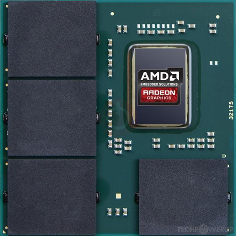
GPU
Recommended Gaming Resolutions:
- 1600x900
- 1920x1080
- 2560x1440
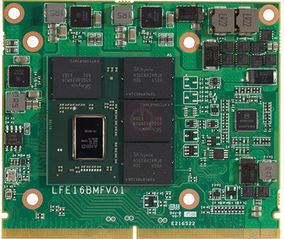
The Radeon E9171 MCM was a mobile graphics chip by AMD, launched on October 3rd, 2017. Built on the 14 nm process, and based on the Lexa graphics processor, in its Lexa MCM Pro variant, the chip supports DirectX 12. This ensures that all modern games will run on Radeon E9171 MCM. The Lexa graphics processor is an average sized chip with a die area of 103 mm² and 2,200 million transistors. Unlike the fully unlocked Radeon 550X 640SP, which uses the same GPU but has all 640 shaders enabled, AMD has disabled some shading units on the Radeon E9171 MCM to reach the product's target shader count. It features 512 shading units, 32 texture mapping units, and 16 ROPs. AMD has paired 4 GB GDDR5 memory with the Radeon E9171 MCM, which are connected using a 128-bit memory interface. The GPU is operating at a frequency of 1124 MHz, which can be boosted up to 1219 MHz, memory is running at 1500 MHz (6 Gbps effective).
Its power draw is rated at 40 W maximum. This device has no display connectivity, as it is not designed to have monitors connected to it. Rather it is intended for use in laptop/notebooks and will use the output of the host mobile device. Radeon E9171 MCM is connected to the rest of the system using a PCI-Express 3.0 x8 interface.
Its power draw is rated at 40 W maximum. This device has no display connectivity, as it is not designed to have monitors connected to it. Rather it is intended for use in laptop/notebooks and will use the output of the host mobile device. Radeon E9171 MCM is connected to the rest of the system using a PCI-Express 3.0 x8 interface.
Graphics Processor
Mobile Graphics
- Release Date
- Oct 3rd, 2017
- Generation
-
Embedded
(9000)
- Production
- End-of-life
- Bus Interface
- PCIe 3.0 x8
Relative Performance
Based on TPU review data: "Performance Summary" at 1920x1080, 4K for 2080 Ti and faster.
Performance estimated based on architecture, shader count and clocks.
Clock Speeds
- Base Clock
- 1124 MHz
- Boost Clock
- 1219 MHz
- Memory Clock
-
1500 MHz
6 Gbps effective
Memory
- Memory Size
- 4 GB
- Memory Type
- GDDR5
- Memory Bus
- 128 bit
- Bandwidth
- 96.00 GB/s
Render Config
- Shading Units
- 512
- TMUs
- 32
- ROPs
- 16
- Compute Units
- 8
- L1 Cache
- 16 KB (per CU)
- L2 Cache
- 512 KB
Theoretical Performance
- Pixel Rate
- 19.50 GPixel/s
- Texture Rate
- 39.01 GTexel/s
- FP16 (half)
- 1,248 GFLOPS (1:1)
- FP32 (float)
- 1,248 GFLOPS
- FP64 (double)
- 78.02 GFLOPS (1:16)
Board Design
- Slot Width
- IGP
- TDP
- 40 W
- Outputs
- Portable Device Dependent
- Power Connectors
- None
Graphics Features
- DirectX
- 12 (12_0)
- OpenGL
- 4.6
- OpenCL
- 2.1
- Vulkan
- 1.3
- Shader Model
- 6.7
Lexa GPU Notes
| Generation: Arctic Islands Codename: Polaris 12 Old Codename: Treasure Graphics/Compute: GFX8 (gfx804) Display Core Engine: 11.2 Unified Video Decoder: 6.3 Video Compression Engine: 3.4 System DMA: 3.0.0 CLRX: GCN 1.2.0 |
Apr 23rd, 2024 15:57 EDT
change timezone
Latest GPU Drivers
New Forum Posts
- Aida64 cache mem OC (0)
- windows 11 (4)
- Which new games will you be buying? (299)
- Meta Horizon OS (5)
- No POST, and no display (6)
- need help with motherboard/ ram compability certainty (5)
- My computer setup - Request for opinions (11)
- EK seems to be having major issues (26)
- DeepCool AIO LS720 RGB NOT WORKING HELP! (0)
- Is there a technical reason that Windows 11 doesn't have built into it battery charge limitation? (36)
Popular Reviews
- Horizon Forbidden West Performance Benchmark Review - 30 GPUs Tested
- Fractal Design Terra Review
- Corsair 2000D Airflow Review
- Thermalright Phantom Spirit 120 EVO Review
- Minisforum EliteMini UM780 XTX (AMD Ryzen 7 7840HS) Review
- ASUS GeForce RTX 4090 STRIX OC Review
- NVIDIA GeForce RTX 4090 Founders Edition Review - Impressive Performance
- ASUS GeForce RTX 4090 Matrix Platinum Review - The RTX 4090 Ti
- Creative Pebble X Plus Review
- MSI GeForce RTX 4090 Gaming X Trio Review
Controversial News Posts
- Sony PlayStation 5 Pro Specifications Confirmed, Console Arrives Before Holidays (116)
- NVIDIA Points Intel Raptor Lake CPU Users to Get Help from Intel Amid System Instability Issues (105)
- AMD "Strix Halo" Zen 5 Mobile Processor Pictured: Chiplet-based, Uses 256-bit LPDDR5X (101)
- US Government Wants Nuclear Plants to Offload AI Data Center Expansion (98)
- Windows 10 Security Updates to Cost $61 After 2025, $427 by 2028 (84)
- Developers of Outpost Infinity Siege Recommend Underclocking i9-13900K and i9-14900K for Stability on Machines with RTX 4090 (84)
- TechPowerUp Hiring: Reviewers Wanted for Motherboards, Laptops, Gaming Handhelds and Prebuilt Desktops (74)
- Intel Realizes the Only Way to Save x86 is to Democratize it, Reopens x86 IP Licensing (70)