Report an Error


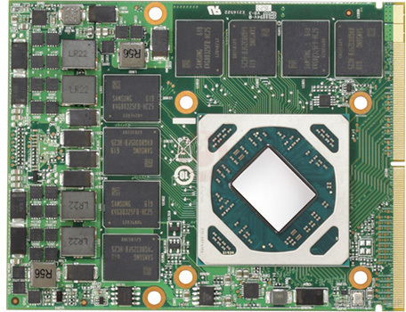
AMD Radeon E9550 MXM
- Graphics Processor
- Ellesmere
- Cores
- 2304
- TMUs
- 144
- ROPs
- 32
- Memory Size
- 8 GB
- Memory Type
- GDDR5
- Bus Width
- 256 bit

GPU
Recommended Gaming Resolutions:
- 1920x1080
- 2560x1440
- 3840x2160
The Radeon E9550 MXM is a mobile graphics chip by AMD, launched on September 27th, 2016. Built on the 14 nm process, and based on the Ellesmere graphics processor, in its Polaris 10 E9550 variant, the chip supports DirectX 12. This ensures that all modern games will run on Radeon E9550 MXM. The Ellesmere graphics processor is an average sized chip with a die area of 232 mm² and 5,700 million transistors. It features 2304 shading units, 144 texture mapping units, and 32 ROPs. AMD has paired 8 GB GDDR5 memory with the Radeon E9550 MXM, which are connected using a 256-bit memory interface. The GPU is operating at a frequency of 1120 MHz, which can be boosted up to 1244 MHz, memory is running at 1250 MHz (5 Gbps effective).
Being a mxm module card, the AMD Radeon E9550 MXM does not require any additional power connector, its power draw is rated at 95 W maximum. Display outputs include: 1x HDMI 2.0b, 3x DisplayPort 1.4a.
Being a mxm module card, the AMD Radeon E9550 MXM does not require any additional power connector, its power draw is rated at 95 W maximum. Display outputs include: 1x HDMI 2.0b, 3x DisplayPort 1.4a.
Graphics Processor
Mobile Graphics
Relative Performance
Based on TPU review data: "Performance Summary" at 1920x1080, 4K for 2080 Ti and faster.
Performance estimated based on architecture, shader count and clocks.
Clock Speeds
- Base Clock
- 1120 MHz
- Boost Clock
- 1244 MHz
- Memory Clock
-
1250 MHz
5 Gbps effective
Memory
- Memory Size
- 8 GB
- Memory Type
- GDDR5
- Memory Bus
- 256 bit
- Bandwidth
- 160.0 GB/s
Render Config
- Shading Units
- 2304
- TMUs
- 144
- ROPs
- 32
- Compute Units
- 36
- L1 Cache
- 16 KB (per CU)
- L2 Cache
- 2 MB
Theoretical Performance
- Pixel Rate
- 39.81 GPixel/s
- Texture Rate
- 179.1 GTexel/s
- FP16 (half)
- 5.732 TFLOPS (1:1)
- FP32 (float)
- 5.732 TFLOPS
- FP64 (double)
- 358.3 GFLOPS (1:16)
Board Design
- Slot Width
- MXM Module
- TDP
- 95 W
- Outputs
- 1x HDMI 2.0b
3x DisplayPort 1.4a
- Power Connectors
- None
Graphics Features
- DirectX
- 12 (12_0)
- OpenGL
- 4.6
- OpenCL
- 2.1
- Vulkan
- 1.3
- Shader Model
- 6.7
Ellesmere GPU Notes
| Generation: Arctic Islands Codename: Polaris 10/20/30 Old Codename: Cozumel / Hawaii Refresh Graphics/Compute: GFX8 (gfx803) Display Core Engine: 11.2 Unified Video Decoder: 6.3 Video Compression Engine: 3.4 System DMA: 3.0.0 CLRX: GCN 1.2.0 |
Apr 25th, 2024 18:43 EDT
change timezone
Latest GPU Drivers
New Forum Posts
- Alphacool CORE 1 CPU block - bulging with danger of splitting? (16)
- Core PL1 + GPU PL1 + Ring EDP OTHER (7)
- How to check flatness of CPUs and coolers - INK and OPTICAL INTERFERENCE methods (112)
- Best SSD for system drive (78)
- Which new games will you be buying? (314)
- TPU's Nostalgic Hardware Club (18464)
- Post your Cinebench 2024 score (450)
- Ubuntu 24.04 LTS released (2)
- Dell Workstation Owners Club (3054)
- im new to throttelstop and i think i messed it up by copying others any hints would be very much aprreciated (2)
Popular Reviews
- Fractal Design Terra Review
- Thermalright Phantom Spirit 120 EVO Review
- Corsair 2000D Airflow Review
- Minisforum EliteMini UM780 XTX (AMD Ryzen 7 7840HS) Review
- ASUS GeForce RTX 4090 STRIX OC Review
- NVIDIA GeForce RTX 4090 Founders Edition Review - Impressive Performance
- ASUS GeForce RTX 4090 Matrix Platinum Review - The RTX 4090 Ti
- MSI GeForce RTX 4090 Suprim X Review
- MSI GeForce RTX 4090 Gaming X Trio Review
- Gigabyte GeForce RTX 4090 Gaming OC Review
Controversial News Posts
- Sony PlayStation 5 Pro Specifications Confirmed, Console Arrives Before Holidays (117)
- Windows 11 Now Officially Adware as Microsoft Embeds Ads in the Start Menu (106)
- NVIDIA Points Intel Raptor Lake CPU Users to Get Help from Intel Amid System Instability Issues (106)
- AMD "Strix Halo" Zen 5 Mobile Processor Pictured: Chiplet-based, Uses 256-bit LPDDR5X (101)
- US Government Wants Nuclear Plants to Offload AI Data Center Expansion (98)
- AMD's RDNA 4 GPUs Could Stick with 18 Gbps GDDR6 Memory (87)
- Developers of Outpost Infinity Siege Recommend Underclocking i9-13900K and i9-14900K for Stability on Machines with RTX 4090 (85)
- Windows 10 Security Updates to Cost $61 After 2025, $427 by 2028 (84)