Report an Error


AMD Radeon HD 6470M
- Graphics Processor
- Seymour
- Cores
- 160
- TMUs
- 8
- ROPs
- 4
- Memory Size
- 512 MB
- Memory Type
- DDR3
- Bus Width
- 64 bit

GPU
Recommended Gaming Resolutions:
- 640x480
- 1280x720
- 1366x768
The Radeon HD 6470M was a mobile graphics chip by AMD, launched on January 4th, 2011. Built on the 40 nm process, and based on the Seymour graphics processor, in its Seymour XT M2 variant, the chip supports DirectX 11.2. The Seymour graphics processor is a relatively small chip with a die area of only 67 mm² and 370 million transistors. It features 160 shading units, 8 texture mapping units, and 4 ROPs. AMD has paired 512 MB DDR3 memory with the Radeon HD 6470M, which are connected using a 64-bit memory interface. The GPU is operating at a frequency of 700 MHz, memory is running at 800 MHz.
Its power draw is rated at 25 W maximum. This device has no display connectivity, as it is not designed to have monitors connected to it. Rather it is intended for use in laptop/notebooks and will use the output of the host mobile device. Radeon HD 6470M is connected to the rest of the system using a PCI-Express 2.0 x16 interface.
Its power draw is rated at 25 W maximum. This device has no display connectivity, as it is not designed to have monitors connected to it. Rather it is intended for use in laptop/notebooks and will use the output of the host mobile device. Radeon HD 6470M is connected to the rest of the system using a PCI-Express 2.0 x16 interface.
Graphics Processor
- GPU Name
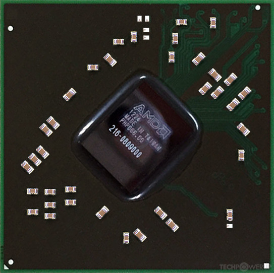
- Seymour
- GPU Variant
-
Seymour XT M2
(216-0809000)
- Architecture
- TeraScale 2
- Foundry
- TSMC
- Process Size
- 40 nm
- Transistors
- 370 million
- Density
- 5.5M / mm²
- Die Size
- 67 mm²
- Chip Package
- FCBGA-631/962
Mobile Graphics
Relative Performance
Based on TPU review data: "Performance Summary" at 1920x1080, 4K for 2080 Ti and faster.
Performance estimated based on architecture, shader count and clocks.
Clock Speeds
- GPU Clock
- 700 MHz
- Memory Clock
-
800 MHz
1600 Mbps effective
Memory
- Memory Size
- 512 MB
- Memory Type
- DDR3
- Memory Bus
- 64 bit
- Bandwidth
- 12.80 GB/s
Render Config
- Shading Units
- 160
- TMUs
- 8
- ROPs
- 4
- Compute Units
- 2
- L1 Cache
- 8 KB (per CU)
- L2 Cache
- 128 KB
Theoretical Performance
- Pixel Rate
- 2.800 GPixel/s
- Texture Rate
- 5.600 GTexel/s
- FP32 (float)
- 224.0 GFLOPS
Board Design
- TDP
- 25 W
- Outputs
- Portable Device Dependent
Graphics Features
- DirectX
- 11.2 (11_0)
- OpenGL
- 4.4
- OpenCL
- 1.2
- Vulkan
- N/A
- Shader Model
- 5.0
Card Notes
| Common alternative clocks are 750MHz core and/or 900MHz memory. |
Seymour GPU Notes
| Generation: Northern Islands Desktop Variant: Caicos Graphics/Compute: GFX4 Display Core Engine: 5.0 Unified Video Decoder: 3.1 |
Devices based on this design (2)
| Name | GPU Clock | Memory Clock | Other Changes |
|---|---|---|---|
| 750 MHz | 900 MHz | 1024 MB | |
| 700 MHz | 800 MHz | 1024 MB |


Apr 23rd, 2024 12:02 EDT
change timezone
Latest GPU Drivers
New Forum Posts
- FINAL FANTASY XIV: Dawntrail Official Benchmark (65)
- Is there a technical reason that Windows 11 doesn't have built into it battery charge limitation? (30)
- What's your latest tech purchase? (20298)
- Asus Crosshair X670E - CPU Package temps (10)
- Core PL1 + GPU PL1 + Ring EDP OTHER (4)
- 5.1 or 7.1 software solutions (1)
- SOYO RX580 2048SP Original Bios (8)
- Unlock the shaders - AMD Radeon RX 560D (323)
- Possible near-future 2024 Arrow Lake build.... (49)
- What are you playing? (20521)
Popular Reviews
- Horizon Forbidden West Performance Benchmark Review - 30 GPUs Tested
- Fractal Design Terra Review
- Corsair 2000D Airflow Review
- Thermalright Phantom Spirit 120 EVO Review
- Minisforum EliteMini UM780 XTX (AMD Ryzen 7 7840HS) Review
- ASUS GeForce RTX 4090 STRIX OC Review
- NVIDIA GeForce RTX 4090 Founders Edition Review - Impressive Performance
- ASUS GeForce RTX 4090 Matrix Platinum Review - The RTX 4090 Ti
- Creative Pebble X Plus Review
- MSI GeForce RTX 4090 Gaming X Trio Review
Controversial News Posts
- Sony PlayStation 5 Pro Specifications Confirmed, Console Arrives Before Holidays (116)
- NVIDIA Points Intel Raptor Lake CPU Users to Get Help from Intel Amid System Instability Issues (105)
- AMD "Strix Halo" Zen 5 Mobile Processor Pictured: Chiplet-based, Uses 256-bit LPDDR5X (101)
- US Government Wants Nuclear Plants to Offload AI Data Center Expansion (98)
- Windows 10 Security Updates to Cost $61 After 2025, $427 by 2028 (84)
- Developers of Outpost Infinity Siege Recommend Underclocking i9-13900K and i9-14900K for Stability on Machines with RTX 4090 (82)
- TechPowerUp Hiring: Reviewers Wanted for Motherboards, Laptops, Gaming Handhelds and Prebuilt Desktops (74)
- Intel Realizes the Only Way to Save x86 is to Democratize it, Reopens x86 IP Licensing (70)