Report an Error


AMD Radeon RX 470D
- Graphics Processor
- Ellesmere
- Cores
- 1792
- TMUs
- 112
- ROPs
- 32
- Memory Size
- 4 GB
- Memory Type
- GDDR5
- Bus Width
- 256 bit

GPU
Recommended Gaming Resolutions:
- 1920x1080
- 2560x1440
- 3840x2160
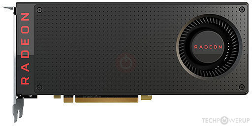
The Radeon RX 470D is a graphics card by AMD, launched on October 21st, 2016. Built on the 14 nm process, and based on the Ellesmere graphics processor, in its Polaris 10 PROD variant, the card supports DirectX 12. This ensures that all modern games will run on Radeon RX 470D. The Ellesmere graphics processor is an average sized chip with a die area of 232 mm² and 5,700 million transistors. Unlike the fully unlocked Radeon RX 480, which uses the same GPU but has all 2304 shaders enabled, AMD has disabled some shading units on the Radeon RX 470D to reach the product's target shader count. It features 1792 shading units, 112 texture mapping units, and 32 ROPs. AMD has paired 4 GB GDDR5 memory with the Radeon RX 470D, which are connected using a 256-bit memory interface. The GPU is operating at a frequency of 926 MHz, which can be boosted up to 1206 MHz, memory is running at 1650 MHz (6.6 Gbps effective).
Being a dual-slot card, the AMD Radeon RX 470D draws power from 1x 6-pin power connector, with power draw rated at 120 W maximum. Display outputs include: 1x HDMI 2.0b, 3x DisplayPort 1.4a. Radeon RX 470D is connected to the rest of the system using a PCI-Express 3.0 x16 interface. The card measures 241 mm in length, and features a dual-slot cooling solution.
Being a dual-slot card, the AMD Radeon RX 470D draws power from 1x 6-pin power connector, with power draw rated at 120 W maximum. Display outputs include: 1x HDMI 2.0b, 3x DisplayPort 1.4a. Radeon RX 470D is connected to the rest of the system using a PCI-Express 3.0 x16 interface. The card measures 241 mm in length, and features a dual-slot cooling solution.
Graphics Processor
Graphics Card
- Release Date
- Oct 21st, 2016
- Generation
-
Arctic Islands
(RX 400)
- Predecessor
- Pirate Islands
- Successor
- Polaris
- Production
- Active
- Bus Interface
- PCIe 3.0 x16
Relative Performance
Based on TPU review data: "Performance Summary" at 1920x1080, 4K for 2080 Ti and faster.
Performance estimated based on architecture, shader count and clocks.
Clock Speeds
- Base Clock
- 926 MHz
- Boost Clock
- 1206 MHz
- Memory Clock
-
1650 MHz
6.6 Gbps effective
Memory
- Memory Size
- 4 GB
- Memory Type
- GDDR5
- Memory Bus
- 256 bit
- Bandwidth
- 211.2 GB/s
Render Config
- Shading Units
- 1792
- TMUs
- 112
- ROPs
- 32
- Compute Units
- 28
- L1 Cache
- 16 KB (per CU)
- L2 Cache
- 2 MB
Theoretical Performance
- Pixel Rate
- 38.59 GPixel/s
- Texture Rate
- 135.1 GTexel/s
- FP16 (half)
- 4.322 TFLOPS (1:1)
- FP32 (float)
- 4.322 TFLOPS
- FP64 (double)
- 270.1 GFLOPS (1:16)
Board Design
- Slot Width
- Dual-slot
- Length
- 241 mm
9.5 inches
- TDP
- 120 W
- Suggested PSU
- 300 W
- Outputs
- 1x HDMI 2.0b
3x DisplayPort 1.4a
- Power Connectors
- 1x 6-pin
- Board Number
- D000
Graphics Features
- DirectX
- 12 (12_0)
- OpenGL
- 4.6
- OpenCL
- 2.1
- Vulkan
- 1.3
- Shader Model
- 6.7
Card Notes
| Chinese Market Only. |
Ellesmere GPU Notes
| Generation: Arctic Islands Codename: Polaris 10/20/30 Old Codename: Cozumel / Hawaii Refresh Graphics/Compute: GFX8 (gfx803) Display Core Engine: 11.2 Unified Video Decoder: 6.3 Video Compression Engine: 3.4 System DMA: 3.0.0 CLRX: GCN 1.2.0 |
Retail boards based on this design (7)
| Name | GPU Clock | Boost Clock | Memory Clock | Other Changes |
|---|---|---|---|---|
| 926 MHz | 1206 MHz | 1750 MHz | 1x DVI 1x HDMI 3x DisplayPort | |
| 926 MHz | 1206 MHz | 1650 MHz | 240 mm/9.4 inches | |
| 926 MHz | 1226 MHz | 1650 MHz | ||
| 926 MHz | 1206 MHz | 1650 MHz | ||
| 926 MHz | 1216 MHz | 1650 MHz | 173 mm/6.8 inches, 1x DVI 1x HDMI 1x DisplayPort | |
| 926 MHz | 1226 MHz | 1650 MHz | ||
| 926 MHz | 1206 MHz | 1650 MHz | 240 mm/9.4 inches, 2x DVI 1x HDMI 1x DisplayPort |


Apr 23rd, 2024 17:12 EDT
change timezone
Latest GPU Drivers
New Forum Posts
- need help with motherboard/ ram compability certainty (8)
- FINAL FANTASY XIV: Dawntrail Official Benchmark (71)
- ThrottleStop 9.6 Voltage won't change (0)
- CPB Enabled Boot Loop (8)
- No POST, and no display (8)
- Aida64 cache mem OC (5)
- hacked (72)
- Meta Horizon OS (6)
- windows 11 (4)
- Which new games will you be buying? (299)
Popular Reviews
- Horizon Forbidden West Performance Benchmark Review - 30 GPUs Tested
- Fractal Design Terra Review
- Corsair 2000D Airflow Review
- Thermalright Phantom Spirit 120 EVO Review
- Minisforum EliteMini UM780 XTX (AMD Ryzen 7 7840HS) Review
- ASUS GeForce RTX 4090 STRIX OC Review
- NVIDIA GeForce RTX 4090 Founders Edition Review - Impressive Performance
- ASUS GeForce RTX 4090 Matrix Platinum Review - The RTX 4090 Ti
- Creative Pebble X Plus Review
- MSI GeForce RTX 4090 Gaming X Trio Review
Controversial News Posts
- Sony PlayStation 5 Pro Specifications Confirmed, Console Arrives Before Holidays (116)
- NVIDIA Points Intel Raptor Lake CPU Users to Get Help from Intel Amid System Instability Issues (106)
- AMD "Strix Halo" Zen 5 Mobile Processor Pictured: Chiplet-based, Uses 256-bit LPDDR5X (101)
- US Government Wants Nuclear Plants to Offload AI Data Center Expansion (98)
- Windows 10 Security Updates to Cost $61 After 2025, $427 by 2028 (84)
- Developers of Outpost Infinity Siege Recommend Underclocking i9-13900K and i9-14900K for Stability on Machines with RTX 4090 (84)
- TechPowerUp Hiring: Reviewers Wanted for Motherboards, Laptops, Gaming Handhelds and Prebuilt Desktops (74)
- Intel Realizes the Only Way to Save x86 is to Democratize it, Reopens x86 IP Licensing (70)