Report an Error


NVIDIA RTX A2000 12 GB
- Graphics Processor
- GA106
- Cores
- 3328
- TMUs
- 104
- ROPs
- 48
- Memory Size
- 12 GB
- Memory Type
- GDDR6
- Bus Width
- 192 bit

GPU
Recommended Gaming Resolutions:
- 1920x1080
- 2560x1440
- 3840x2160
The RTX A2000 12 GB is a high-end professional graphics card by NVIDIA, launched on November 23rd, 2021. Built on the 8 nm process, and based on the GA106 graphics processor, the card supports DirectX 12 Ultimate. The GA106 graphics processor is an average sized chip with a die area of 276 mm² and 12,000 million transistors. Unlike the fully unlocked GeForce RTX 3060 3840SP, which uses the same GPU but has all 3840 shaders enabled, NVIDIA has disabled some shading units on the RTX A2000 12 GB to reach the product's target shader count. It features 3328 shading units, 104 texture mapping units, and 48 ROPs. Also included are 104 tensor cores which help improve the speed of machine learning applications. The card also has 26 raytracing acceleration cores. NVIDIA has paired 12 GB GDDR6 memory with the RTX A2000 12 GB, which are connected using a 192-bit memory interface. The GPU is operating at a frequency of 562 MHz, which can be boosted up to 1200 MHz, memory is running at 1500 MHz (12 Gbps effective).
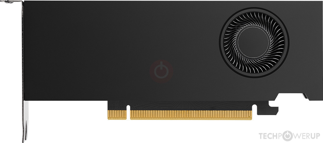
Being a dual-slot card, the NVIDIA RTX A2000 12 GB does not require any additional power connector, its power draw is rated at 70 W maximum. Display outputs include: 4x mini-DisplayPort 1.4a. RTX A2000 12 GB is connected to the rest of the system using a PCI-Express 4.0 x16 interface. The card measures 167 mm in length, 69 mm in width, and features a dual-slot cooling solution. Its price at launch was 449 US Dollars.
Being a dual-slot card, the NVIDIA RTX A2000 12 GB does not require any additional power connector, its power draw is rated at 70 W maximum. Display outputs include: 4x mini-DisplayPort 1.4a. RTX A2000 12 GB is connected to the rest of the system using a PCI-Express 4.0 x16 interface. The card measures 167 mm in length, 69 mm in width, and features a dual-slot cooling solution. Its price at launch was 449 US Dollars.
Graphics Processor
Graphics Card
- Release Date
- Nov 23rd, 2021
- Generation
-
Quadro Ampere
(Ax000)
- Predecessor
- Quadro Turing
- Successor
- Quadro Ada
- Production
- Active
- Launch Price
- 449 USD
- Bus Interface
- PCIe 4.0 x16
- Reviews
- 1 in our database
Relative Performance
Based on TPU review data: "Performance Summary" at 1920x1080, 4K for 2080 Ti and faster.
Performance estimated based on architecture, shader count and clocks.
Clock Speeds
- Base Clock
- 562 MHz
- Boost Clock
- 1200 MHz
- Memory Clock
-
1500 MHz
12 Gbps effective
Memory
- Memory Size
- 12 GB
- Memory Type
- GDDR6
- Memory Bus
- 192 bit
- Bandwidth
- 288.0 GB/s
Render Config
- Shading Units
- 3328
- TMUs
- 104
- ROPs
- 48
- SM Count
- 26
- Tensor Cores
- 104
- RT Cores
- 26
- L1 Cache
- 128 KB (per SM)
- L2 Cache
- 3 MB
Theoretical Performance
- Pixel Rate
- 57.60 GPixel/s
- Texture Rate
- 124.8 GTexel/s
- FP16 (half)
- 7.987 TFLOPS (1:1)
- FP32 (float)
- 7.987 TFLOPS
- FP64 (double)
- 124.8 GFLOPS (1:64)
Board Design
- Slot Width
- Dual-slot
- Length
- 167 mm
6.6 inches
- Width
- 69 mm
2.7 inches
- TDP
- 70 W
- Suggested PSU
- 250 W
- Outputs
- 4x mini-DisplayPort 1.4a
- Power Connectors
- None
- Board Number
- PG192 SKU 510
Graphics Features
- DirectX
- 12 Ultimate (12_2)
- OpenGL
- 4.6
- OpenCL
- 3.0
- Vulkan
- 1.3
- CUDA
- 8.6
- Shader Model
- 6.7
GA106 GPU Notes
| Ray Tracing Cores: 2nd Gen Tensor Cores: 3rd Gen NVENC: 7th Gen NVDEC: 5th Gen PureVideo HD: VP11 VDPAU: Feature Set K |
Apr 24th, 2024 21:59 EDT
change timezone
Latest GPU Drivers
New Forum Posts
- I am getting artifacting when I change Windows security settings. Is my GPU failing, or is this just a Windows issue? (10)
- Is there a technical reason that Windows 11 doesn't have built into it battery charge limitation? (42)
- (Anti) SFF fun house (347)
- Cinebench crashed my PC. My Wi-Fi stopped working, and I keep getting a "Please wait" screen when I boot up my PC. (30)
- The TPU UK Clubhouse (24783)
- Sharing experience with MSI RTX 3070 vBIOS update to enable Resizable Bar with MB Z490 (2)
- Share your AIDA 64 cache and memory benchmark here (2915)
- Will a RTX 4070 TI super bottleneck a Ryzen 9 7950X3D? (58)
- The best *budget* ATX PC case on the market? (24)
- GTX 1070 Ti - TDP Issues - Always Power Throttling (4)
Popular Reviews
- Fractal Design Terra Review
- Thermalright Phantom Spirit 120 EVO Review
- Corsair 2000D Airflow Review
- Minisforum EliteMini UM780 XTX (AMD Ryzen 7 7840HS) Review
- ASUS GeForce RTX 4090 STRIX OC Review
- NVIDIA GeForce RTX 4090 Founders Edition Review - Impressive Performance
- ASUS GeForce RTX 4090 Matrix Platinum Review - The RTX 4090 Ti
- MSI GeForce RTX 4090 Suprim X Review
- Gigabyte GeForce RTX 4090 Gaming OC Review
- MSI GeForce RTX 4090 Gaming X Trio Review
Controversial News Posts
- Sony PlayStation 5 Pro Specifications Confirmed, Console Arrives Before Holidays (116)
- NVIDIA Points Intel Raptor Lake CPU Users to Get Help from Intel Amid System Instability Issues (106)
- AMD "Strix Halo" Zen 5 Mobile Processor Pictured: Chiplet-based, Uses 256-bit LPDDR5X (101)
- US Government Wants Nuclear Plants to Offload AI Data Center Expansion (98)
- Windows 10 Security Updates to Cost $61 After 2025, $427 by 2028 (84)
- Developers of Outpost Infinity Siege Recommend Underclocking i9-13900K and i9-14900K for Stability on Machines with RTX 4090 (84)
- TechPowerUp Hiring: Reviewers Wanted for Motherboards, Laptops, Gaming Handhelds and Prebuilt Desktops (78)
- AMD's RDNA 4 GPUs Could Stick with 18 Gbps GDDR6 Memory (73)