Report an Error


Sapphire HD 4650 HyperMemory 1 GB
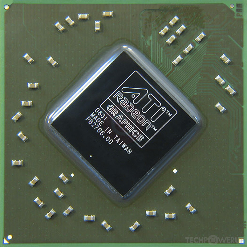
- Graphics Processor
- RV730
- Cores
- 320
- TMUs
- 32
- ROPs
- 8
- Memory Size
- 1024 MB
- Memory Type
- DDR2
- Bus Width
- 128 bit

GPU
Graphics Processor
Graphics Card
- Release Date
Sep 10th, 2008
Dec 4th, 2009
- Generation
-
Radeon R700
(HD 4600)
- Predecessor
- Radeon R600
- Successor
- Evergreen
- Production
- End-of-life
- Bus Interface
- PCIe 2.0 x16
Clock Speeds
- GPU Clock
- 600 MHz
- Memory Clock
-
700 MHz
400 MHz (-43%)
1400 Mbps effective
800 Mbps effective
Memory
- Memory Size
-
256 MB
1024 MB
- Memory Type
GDDR3
DDR2
- Memory Bus
- 128 bit
- Bandwidth
-
22.40 GB/s
12.80 GB/s
Render Config
- Shading Units
- 320
- TMUs
- 32
- ROPs
- 8
- Compute Units
- 4
- L1 Cache
- 16 KB (per CU)
- L2 Cache
- 128 KB
Theoretical Performance
- Pixel Rate
- 4.800 GPixel/s
- Texture Rate
- 19.20 GTexel/s
- FP32 (float)
- 384.0 GFLOPS
Board Design
- Slot Width
- Single-slot
- TDP
- 48 W
- Suggested PSU
- 200 W
- Outputs
2x DVI
1x S-Video
1x DVI
1x VGA
1x S-Video
- Power Connectors
- None
- Board Number
- B668
Graphics Features
- DirectX
- 10.1 (10_1)
- OpenGL
- 3.3
- OpenCL
- 1.1
- Vulkan
- N/A
- Shader Model
- 4.1
RV730 GPU Notes
| Mobile Variant: M96 Codename: Mario Graphics/Compute: GFX3 Display Core Engine: 3.2 Unified Video Decoder: 2.2 |
Other retail boards based on this design (8)
| Name | GPU Clock | Memory Clock | Other Changes |
|---|---|---|---|
| 600 MHz | 700 MHz | 1x DVI 1x VGA | |
| 600 MHz | 400 MHz | 512 MB, DDR2, 1x DVI 1x HDMI 1x VGA | |
| 600 MHz | 500 MHz | 512 MB, DDR2, 1x DVI 1x VGA 1x S-Video, 64 bit | |
| 600 MHz | 700 MHz | 512 MB, 1x DVI 1x HDMI 1x VGA | |
| 600 MHz | 400 MHz | 512 MB, DDR2, 1x DVI 1x VGA 1x S-Video | |
|
Sapphire HD 4650 HyperMemory 1 GB

|
600 MHz | 400 MHz | 1024 MB, DDR2, 1x DVI 1x VGA 1x S-Video |
| 600 MHz | 400 MHz | 512 MB, DDR2, 1x DVI 1x HDMI 1x VGA | |
| 600 MHz | 400 MHz | 1024 MB, DDR2, 1x DVI 1x HDMI 1x VGA |


Apr 24th, 2024 19:58 EDT
change timezone
Latest GPU Drivers
New Forum Posts
- Sharing experience with MSI RTX 3070 vBIOS update to enable Resizable Bar with MB Z490 (2)
- Share your AIDA 64 cache and memory benchmark here (2915)
- Will a RTX 4070 TI super bottleneck a Ryzen 9 7950X3D? (58)
- The best *budget* ATX PC case on the market? (24)
- GTX 1070 Ti - TDP Issues - Always Power Throttling (4)
- The TPU UK Clubhouse (24782)
- 2022-X58/1366 PIN Motherboards NVME M.2 SSD BIOS MOD Collection (656)
- Meta Horizon OS (15)
- Is there a technical reason that Windows 11 doesn't have built into it battery charge limitation? (41)
- Best SSD for system drive (75)
Popular Reviews
- Fractal Design Terra Review
- Thermalright Phantom Spirit 120 EVO Review
- Corsair 2000D Airflow Review
- Minisforum EliteMini UM780 XTX (AMD Ryzen 7 7840HS) Review
- ASUS GeForce RTX 4090 STRIX OC Review
- NVIDIA GeForce RTX 4090 Founders Edition Review - Impressive Performance
- ASUS GeForce RTX 4090 Matrix Platinum Review - The RTX 4090 Ti
- MSI GeForce RTX 4090 Gaming X Trio Review
- MSI GeForce RTX 4090 Suprim X Review
- Gigabyte GeForce RTX 4090 Gaming OC Review
Controversial News Posts
- Sony PlayStation 5 Pro Specifications Confirmed, Console Arrives Before Holidays (116)
- NVIDIA Points Intel Raptor Lake CPU Users to Get Help from Intel Amid System Instability Issues (106)
- AMD "Strix Halo" Zen 5 Mobile Processor Pictured: Chiplet-based, Uses 256-bit LPDDR5X (101)
- US Government Wants Nuclear Plants to Offload AI Data Center Expansion (98)
- Windows 10 Security Updates to Cost $61 After 2025, $427 by 2028 (84)
- Developers of Outpost Infinity Siege Recommend Underclocking i9-13900K and i9-14900K for Stability on Machines with RTX 4090 (84)
- TechPowerUp Hiring: Reviewers Wanted for Motherboards, Laptops, Gaming Handhelds and Prebuilt Desktops (78)
- AMD's RDNA 4 GPUs Could Stick with 18 Gbps GDDR6 Memory (71)