Report an Error


NVIDIA Quadro FX 4800
- Graphics Processor
- GT200B
- Cores
- 192
- TMUs
- 64
- ROPs
- 24
- Memory Size
- 1536 MB
- Memory Type
- GDDR3
- Bus Width
- 384 bit

GPU

Bottom

Back
Recommended Gaming Resolutions:
- 1366x768
- 1600x900
- 1920x1080
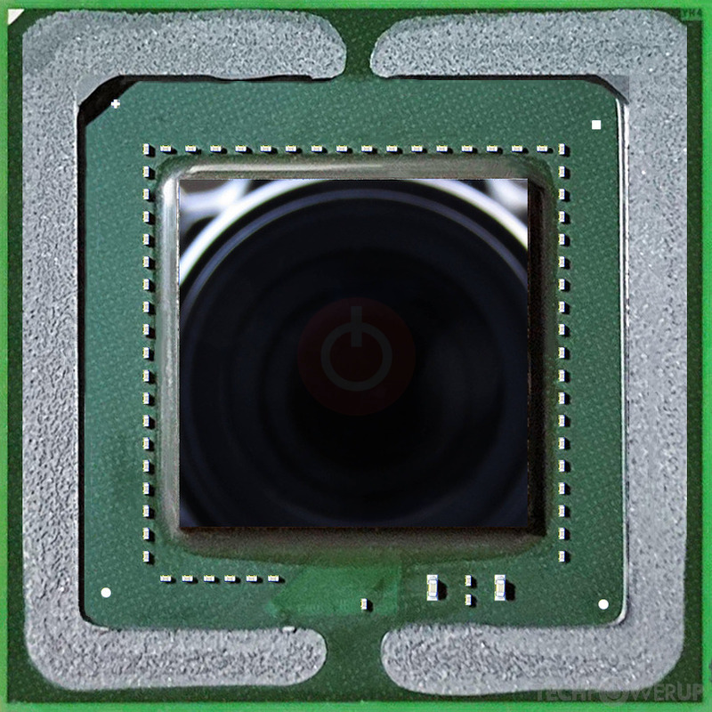
The Quadro FX 4800 was an enthusiast-class professional graphics card by NVIDIA, launched on November 11th, 2008. Built on the 55 nm process, and based on the GT200B graphics processor, the card supports DirectX 11.1. Even though it supports DirectX 11, the feature level is only 10_0, which can be problematic with many DirectX 11 & DirectX 12 titles. The GT200B graphics processor is a large chip with a die area of 470 mm² and 1,400 million transistors. Unlike the fully unlocked GeForce GTX 285, which uses the same GPU but has all 240 shaders enabled, NVIDIA has disabled some shading units on the Quadro FX 4800 to reach the product's target shader count. It features 192 shading units, 64 texture mapping units, and 24 ROPs. NVIDIA has paired 1,536 MB GDDR3 memory with the Quadro FX 4800, which are connected using a 384-bit memory interface. The GPU is operating at a frequency of 602 MHz, memory is running at 800 MHz.
Being a dual-slot card, the NVIDIA Quadro FX 4800 draws power from 1x 6-pin power connector, with power draw rated at 150 W maximum. Display outputs include: 1x DVI, 2x DisplayPort, 1x S-Video. Quadro FX 4800 is connected to the rest of the system using a PCI-Express 2.0 x16 interface. The card measures 267 mm in length, 111 mm in width, and features a dual-slot cooling solution. Its price at launch was 1799 US Dollars.
Being a dual-slot card, the NVIDIA Quadro FX 4800 draws power from 1x 6-pin power connector, with power draw rated at 150 W maximum. Display outputs include: 1x DVI, 2x DisplayPort, 1x S-Video. Quadro FX 4800 is connected to the rest of the system using a PCI-Express 2.0 x16 interface. The card measures 267 mm in length, 111 mm in width, and features a dual-slot cooling solution. Its price at launch was 1799 US Dollars.
Graphics Processor
Graphics Card
- Release Date
- Nov 11th, 2008
- Generation
-
Quadro FX Tesla
(x800)
- Predecessor
- Quadro FX Curie
- Successor
- Quadro Fermi
- Production
- End-of-life
- Launch Price
- 1,799 USD
- Bus Interface
- PCIe 2.0 x16
- Reviews
- 26 in our database
Relative Performance
Based on TPU review data: "Performance Summary" at 1920x1080, 4K for 2080 Ti and faster.
Performance estimated based on architecture, shader count and clocks.
Clock Speeds
- GPU Clock
- 602 MHz
- Shader Clock
- 1204 MHz
- Memory Clock
-
800 MHz
1600 Mbps effective
Memory
- Memory Size
- 1536 MB
- Memory Type
- GDDR3
- Memory Bus
- 384 bit
- Bandwidth
- 76.80 GB/s
Render Config
- Shading Units
- 192
- TMUs
- 64
- ROPs
- 24
- SM Count
- 24
- L2 Cache
- 192 KB
Theoretical Performance
- Pixel Rate
- 14.45 GPixel/s
- Texture Rate
- 38.53 GTexel/s
- FP32 (float)
- 462.3 GFLOPS
- FP64 (double)
- 57.79 GFLOPS (1:8)
Board Design
- Slot Width
- Dual-slot
- Length
- 267 mm
10.5 inches
- Width
- 111 mm
4.4 inches
- TDP
- 150 W
- Suggested PSU
- 450 W
- Outputs
- 1x DVI
2x DisplayPort
1x S-Video
- Power Connectors
- 1x 6-pin
- Board Number
- P607 SKU 501
Graphics Features
- DirectX
- 11.1 (10_0)
- OpenGL
- 3.3
- OpenCL
- 1.1
- Vulkan
- N/A
- CUDA
- 1.3
- Shader Model
- 4.0
GT200B GPU Notes
| PureVideo HD: VP2 VDPAU: Feature Set A GT200B, commonly printed on the chip package as G200-xxx-Bx is an optical shrink of the G200 core to the newer 55 manufacturing process of TSMC. It helped shrink the core's energy and thermal footprints to a level that even facilitated building a dual-GPU accelerator |
Apr 19th, 2024 15:30 EDT
change timezone
Latest GPU Drivers
New Forum Posts
- Will a RTX 4070 TI super bottleneck a Ryzen 9 7950X3D? (39)
- [WIN11] 5700x3d Security processor Attestation: Not supported? (3)
- Is it possible to use Linux without the Terminal/command line? (27)
- Linus watercools (45)
- Which air cooler for a ryzen 9 5900x (160)
- Which terminal emulator do you use the most? (9)
- I9 13890HX undervolting Suggestions (2)
- Whats your favourite Linux Distro? (52)
- DDR5 RAM Speeds and the future (50)
- What can be changed in a VBIOS file? (PCI vendor etc) (4)
Popular Reviews
- Horizon Forbidden West Performance Benchmark Review - 30 GPUs Tested
- PowerColor Radeon RX 7900 GRE Hellhound Review
- Fractal Design Terra Review
- Corsair 2000D Airflow Review
- Thermalright Phantom Spirit 120 EVO Review
- Minisforum EliteMini UM780 XTX (AMD Ryzen 7 7840HS) Review
- Creative Pebble X Plus Review
- FiiO KB3 HiFi Mechanical Keyboard Review - Integrated DAC/Amp!
- ASUS GeForce RTX 4090 STRIX OC Review
- NVIDIA GeForce RTX 4090 Founders Edition Review - Impressive Performance
Controversial News Posts
- Sony PlayStation 5 Pro Specifications Confirmed, Console Arrives Before Holidays (110)
- NVIDIA Points Intel Raptor Lake CPU Users to Get Help from Intel Amid System Instability Issues (102)
- US Government Wants Nuclear Plants to Offload AI Data Center Expansion (98)
- Windows 10 Security Updates to Cost $61 After 2025, $427 by 2028 (82)
- Developers of Outpost Infinity Siege Recommend Underclocking i9-13900K and i9-14900K for Stability on Machines with RTX 4090 (82)
- AMD "Strix Halo" Zen 5 Mobile Processor Pictured: Chiplet-based, Uses 256-bit LPDDR5X (76)
- TechPowerUp Hiring: Reviewers Wanted for Motherboards, Laptops, Gaming Handhelds and Prebuilt Desktops (72)
- Intel Realizes the Only Way to Save x86 is to Democratize it, Reopens x86 IP Licensing (70)