Report an Error


NVIDIA GeForce Go 6600
- Graphics Processor
- NV43
- Pixel Shaders
- 8
- Vertex Shaders
- 3
- TMUs
- 8
- ROPs
- 4
- Memory Size
- 256 MB
- Memory Type
- DDR
- Bus Width
- 128 bit

GPU
Recommended Gaming Resolutions:
- 640x480
- 1280x720
- 1366x768
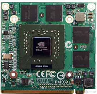
The GeForce Go 6600 was a mobile graphics chip by NVIDIA, launched on September 29th, 2005. Built on the 110 nm process, and based on the NV43 graphics processor, in its NV43M A2 variant, the chip supports DirectX 9.0c. Since GeForce Go 6600 does not support DirectX 11 or DirectX 12, it might not be able to run all the latest games. The NV43 graphics processor is an average sized chip with a die area of 154 mm² and 146 million transistors. It features 8 pixel shaders and 3 vertex shaders, 8 texture mapping units, and 4 ROPs. Due to the lack of unified shaders you will not be able to run recent games at all (which require unified shader/DX10+ support). NVIDIA has paired 256 MB DDR memory with the GeForce Go 6600, which are connected using a 128-bit memory interface. The GPU is operating at a frequency of 300 MHz, memory is running at 350 MHz.
Being a mxm module card, the NVIDIA GeForce Go 6600 does not require any additional power connector, its power draw is not exactly known. This device has no display connectivity, as it is not designed to have monitors connected to it. Rather it is intended for use in laptop/notebooks and will use the output of the host mobile device.
Being a mxm module card, the NVIDIA GeForce Go 6600 does not require any additional power connector, its power draw is not exactly known. This device has no display connectivity, as it is not designed to have monitors connected to it. Rather it is intended for use in laptop/notebooks and will use the output of the host mobile device.
Graphics Processor
Mobile Graphics
- Release Date
- Sep 29th, 2005
- Generation
-
GeForce Go 6
(Go 6000)
- Predecessor
- GeForce FX Go 5
- Successor
- GeForce Go 7
- Production
- End-of-life
- Bus Interface
- MXM-II
- Reviews
- 2 in our database
Clock Speeds
- GPU Clock
- 300 MHz
- Memory Clock
-
350 MHz
700 Mbps effective
Memory
- Memory Size
- 256 MB
- Memory Type
- DDR
- Memory Bus
- 128 bit
- Bandwidth
- 11.20 GB/s
Render Config
- Pixel Shaders
- 8
- Vertex Shaders
- 3
- TMUs
- 8
- ROPs
- 4
Theoretical Performance
- Pixel Rate
- 1.200 GPixel/s
- Vertex Rate
- 225.0 MVertices/s
- Texture Rate
- 2.400 GTexel/s
Board Design
- Slot Width
- MXM Module
- TDP
- unknown
- Outputs
- Portable Device Dependent
- Power Connectors
- None
- Board Number
- E233 SKU 30,
P264 SKU 0
Graphics Features
- DirectX
- 9.0c (9_3)
- OpenGL
-
2.0 (full)
2.1 (partial)
- OpenCL
- N/A
- Vulkan
- N/A
- Shader Model
- 3.0
NV43 GPU Notes
| PureVideo HD: VP1 VDPAU: No Support |
Apr 24th, 2024 15:02 EDT
change timezone
Latest GPU Drivers
New Forum Posts
- Meta Horizon OS (12)
- Will a RTX 4070 TI super bottleneck a Ryzen 9 7950X3D? (53)
- GTX 1070 Ti - TDP Issues - Always Power Throttling (0)
- What are you playing? (20523)
- Youtube layout has changed, how to go back ? (16)
- How are MX330 and İ5 1135G7 ? (8)
- Is there a technical reason that Windows 11 doesn't have built into it battery charge limitation? (40)
- Realtek Modded Audio Driver for Windows 10/11 - Only for HDAUDIO (5690)
- I7-8750H + GTX 1050ti Laptop drops performance periodically (5)
- Aida64 cache mem OC (6)
Popular Reviews
- Fractal Design Terra Review
- Thermalright Phantom Spirit 120 EVO Review
- Corsair 2000D Airflow Review
- Minisforum EliteMini UM780 XTX (AMD Ryzen 7 7840HS) Review
- ASUS GeForce RTX 4090 STRIX OC Review
- NVIDIA GeForce RTX 4090 Founders Edition Review - Impressive Performance
- ASUS GeForce RTX 4090 Matrix Platinum Review - The RTX 4090 Ti
- MSI GeForce RTX 4090 Suprim X Review
- MSI GeForce RTX 4090 Gaming X Trio Review
- Gigabyte GeForce RTX 4090 Gaming OC Review
Controversial News Posts
- Sony PlayStation 5 Pro Specifications Confirmed, Console Arrives Before Holidays (116)
- NVIDIA Points Intel Raptor Lake CPU Users to Get Help from Intel Amid System Instability Issues (106)
- AMD "Strix Halo" Zen 5 Mobile Processor Pictured: Chiplet-based, Uses 256-bit LPDDR5X (101)
- US Government Wants Nuclear Plants to Offload AI Data Center Expansion (98)
- Windows 10 Security Updates to Cost $61 After 2025, $427 by 2028 (84)
- Developers of Outpost Infinity Siege Recommend Underclocking i9-13900K and i9-14900K for Stability on Machines with RTX 4090 (84)
- TechPowerUp Hiring: Reviewers Wanted for Motherboards, Laptops, Gaming Handhelds and Prebuilt Desktops (78)
- Intel Realizes the Only Way to Save x86 is to Democratize it, Reopens x86 IP Licensing (70)