Report an Error


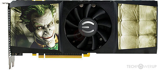
NVIDIA GeForce GTX 275 PhysX Edition
- Graphics Processor
- GT200B
- Cores
- 240
- TMUs
- 80
- ROPs
- 28
- Memory Size
- 896 MB
- Memory Type
- GDDR3
- Bus Width
- 448 bit

GPU
Recommended Gaming Resolutions:
- 1366x768
- 1600x900
- 1920x1080
The GeForce GTX 275 PhysX Edition was a graphics card by NVIDIA, launched on February 16th, 2010. Built on the 55 nm process, and based on the GT200B graphics processor, in its G200-105-B3 variant, the card supports DirectX 11.1. Even though it supports DirectX 11, the feature level is only 10_0, which can be problematic with many DirectX 11 & DirectX 12 titles. The GT200B graphics processor is a large chip with a die area of 470 mm² and 1,400 million transistors. It features 240 shading units, 80 texture mapping units, and 28 ROPs. NVIDIA has paired 896 MB GDDR3 memory with the GeForce GTX 275 PhysX Edition, which are connected using a 448-bit memory interface. The GPU is operating at a frequency of 633 MHz, memory is running at 1134 MHz.
Being a dual-slot card, the NVIDIA GeForce GTX 275 PhysX Edition draws power from 1x 6-pin + 1x 8-pin power connector, with power draw rated at 219 W maximum. Display outputs include: 2x DVI. GeForce GTX 275 PhysX Edition is connected to the rest of the system using a PCI-Express 2.0 x16 interface. The card measures 267 mm in length, 111 mm in width, and features a dual-slot cooling solution.
Being a dual-slot card, the NVIDIA GeForce GTX 275 PhysX Edition draws power from 1x 6-pin + 1x 8-pin power connector, with power draw rated at 219 W maximum. Display outputs include: 2x DVI. GeForce GTX 275 PhysX Edition is connected to the rest of the system using a PCI-Express 2.0 x16 interface. The card measures 267 mm in length, 111 mm in width, and features a dual-slot cooling solution.
Graphics Processor
Graphics Processor
Graphics Card
- Release Date
- Feb 16th, 2010
- Generation
- GeForce 200
- Predecessor
- GeForce 9
- Successor
- GeForce 400
- Production
- End-of-life
- Bus Interface
- PCIe 2.0 x16
- Reviews
- 61 in our database
Relative Performance
Based on TPU review data: "Performance Summary" at 1920x1080, 4K for 2080 Ti and faster.
Performance estimated based on architecture, shader count and clocks.
Clock Speeds
- GPU Clock
- 633 MHz
- Shader Clock
- 1296 MHz
- Memory Clock
-
1134 MHz
2.3 Gbps effective
Memory
- Memory Size
- 896 MB
- Memory Type
- GDDR3
- Memory Bus
- 448 bit
- Bandwidth
- 127.0 GB/s
Render Config
- Shading Units
- 240
- TMUs
- 80
- ROPs
- 28
- SM Count
- 30
- L2 Cache
- 224 KB
Theoretical Performance
- Pixel Rate
- 17.72 GPixel/s
- Texture Rate
- 50.64 GTexel/s
- FP32 (float)
- 622.1 GFLOPS
- FP64 (double)
- 77.76 GFLOPS (1:8)
Board Design
- Slot Width
- Dual-slot
- Length
- 267 mm
10.5 inches
- Width
- 111 mm
4.4 inches
- TDP
- 219 W
- Suggested PSU
- 550 W
- Outputs
- 2x DVI
- Power Connectors
- 1x 6-pin + 1x 8-pin
Graphics Features
- DirectX
- 11.1 (10_0)
- OpenGL
- 3.3
- OpenCL
- 1.1
- Vulkan
- N/A
- CUDA
- 1.3
- Shader Model
- 4.0
Card Notes
| Heterogeneous graphics card consisting of one GTX 275 for main graphics functions and one GTS 250 for PhysX. GTS 250 co-processor specs: 738MHz Core Clock 1836MHz Shader Clock 1100MHz (2200MHz effective) 384MB 192-bit GDDR3 128 Unified Shaders 48 TMUs 12 ROPs Combined FP32 performance of 1,092.1 GFLOPS |
GT200B GPU Notes
| PureVideo HD: VP2 VDPAU: Feature Set A GT200B, commonly printed on the chip package as G200-xxx-Bx is an optical shrink of the G200 core to the newer 55 manufacturing process of TSMC. It helped shrink the core's energy and thermal footprints to a level that even facilitated building a dual-GPU accelerator |
Retail boards based on this design (1)
| Name | GPU Clock | Memory Clock | Other Changes |
|---|---|---|---|
| 633 MHz | 1134 MHz |

Apr 23rd, 2024 11:11 EDT
change timezone
Latest GPU Drivers
New Forum Posts
- Core PL1 + GPU PL1 + Ring EDP OTHER (4)
- 5.1 or 7.1 software solutions (1)
- FINAL FANTASY XIV: Dawntrail Official Benchmark (64)
- What's your latest tech purchase? (20297)
- SOYO RX580 2048SP Original Bios (8)
- Unlock the shaders - AMD Radeon RX 560D (323)
- Possible near-future 2024 Arrow Lake build.... (49)
- What are you playing? (20521)
- Windows 12 (142)
- EK seems to be having major issues (25)
Popular Reviews
- Horizon Forbidden West Performance Benchmark Review - 30 GPUs Tested
- Fractal Design Terra Review
- Corsair 2000D Airflow Review
- Thermalright Phantom Spirit 120 EVO Review
- Minisforum EliteMini UM780 XTX (AMD Ryzen 7 7840HS) Review
- ASUS GeForce RTX 4090 STRIX OC Review
- NVIDIA GeForce RTX 4090 Founders Edition Review - Impressive Performance
- ASUS GeForce RTX 4090 Matrix Platinum Review - The RTX 4090 Ti
- Creative Pebble X Plus Review
- MSI GeForce RTX 4090 Gaming X Trio Review
Controversial News Posts
- Sony PlayStation 5 Pro Specifications Confirmed, Console Arrives Before Holidays (116)
- NVIDIA Points Intel Raptor Lake CPU Users to Get Help from Intel Amid System Instability Issues (105)
- AMD "Strix Halo" Zen 5 Mobile Processor Pictured: Chiplet-based, Uses 256-bit LPDDR5X (101)
- US Government Wants Nuclear Plants to Offload AI Data Center Expansion (98)
- Windows 10 Security Updates to Cost $61 After 2025, $427 by 2028 (84)
- Developers of Outpost Infinity Siege Recommend Underclocking i9-13900K and i9-14900K for Stability on Machines with RTX 4090 (82)
- TechPowerUp Hiring: Reviewers Wanted for Motherboards, Laptops, Gaming Handhelds and Prebuilt Desktops (74)
- Intel Realizes the Only Way to Save x86 is to Democratize it, Reopens x86 IP Licensing (70)