Report an Error


NVIDIA Tesla K20s
- Graphics Processor
- GK110
- Cores
- 2496
- TMUs
- 208
- ROPs
- 40
- Memory Size
- 5 GB
- Memory Type
- GDDR5
- Bus Width
- 320 bit

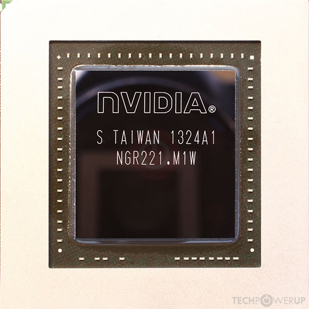
GPU
The Tesla K20s was an enthusiast-class professional graphics card by NVIDIA, launched on February 18th, 2013. Built on the 28 nm process, and based on the GK110 graphics processor, the card supports DirectX 12. The GK110 graphics processor is a large chip with a die area of 561 mm² and 7,080 million transistors. Unlike the fully unlocked GeForce GTX TITAN, which uses the same GPU but has all 2688 shaders enabled, NVIDIA has disabled some shading units on the Tesla K20s to reach the product's target shader count. It features 2496 shading units, 208 texture mapping units, and 40 ROPs. NVIDIA has paired 5 GB GDDR5 memory with the Tesla K20s, which are connected using a 320-bit memory interface. The GPU is operating at a frequency of 575 MHz, memory is running at 1300 MHz (5.2 Gbps effective).
Being a dual-slot card, its power draw is rated at 225 W maximum. This device has no display connectivity, as it is not designed to have monitors connected to it. Tesla K20s is connected to the rest of the system using a PCI-Express 2.0 x16 interface. The card measures 267 mm in length, and features a dual-slot cooling solution. Its price at launch was 3199 US Dollars.
Being a dual-slot card, its power draw is rated at 225 W maximum. This device has no display connectivity, as it is not designed to have monitors connected to it. Tesla K20s is connected to the rest of the system using a PCI-Express 2.0 x16 interface. The card measures 267 mm in length, and features a dual-slot cooling solution. Its price at launch was 3199 US Dollars.
Graphics Processor
Graphics Card
- Release Date
- Feb 18th, 2013
- Generation
-
Tesla Kepler
(Kxx)
- Predecessor
- Tesla Fermi
- Successor
- Tesla Maxwell
- Production
- End-of-life
- Launch Price
- 3,199 USD
- Bus Interface
- PCIe 2.0 x16
Relative Performance
Based on TPU review data: "Performance Summary" at 1920x1080, 4K for 2080 Ti and faster.
Performance estimated based on architecture, shader count and clocks.
Clock Speeds
- GPU Clock
- 575 MHz
- Memory Clock
-
1300 MHz
5.2 Gbps effective
Memory
- Memory Size
- 5 GB
- Memory Type
- GDDR5
- Memory Bus
- 320 bit
- Bandwidth
- 208.0 GB/s
Render Config
- Shading Units
- 2496
- TMUs
- 208
- ROPs
- 40
- SMX Count
- 13
- L1 Cache
- 16 KB (per SMX)
- L2 Cache
- 1280 KB
Theoretical Performance
- Pixel Rate
- 29.90 GPixel/s
- Texture Rate
- 119.6 GTexel/s
- FP32 (float)
- 2.870 TFLOPS
- FP64 (double)
- 956.8 GFLOPS (1:3)
Board Design
- Slot Width
- Dual-slot
- Length
- 267 mm
10.5 inches
- TDP
- 225 W
- Suggested PSU
- 550 W
- Outputs
- No outputs
Graphics Features
- DirectX
- 12 (11_0)
- OpenGL
- 4.6
- OpenCL
- 3.0
- Vulkan
- 1.2.175
- CUDA
- 3.5
- Shader Model
- 6.5 (5.1)
GK110 GPU Notes
| NVENC: 1st Gen NVDEC: 1st Gen PureVideo HD: VP5 VDPAU: Feature Set D L1 Cache is configurable from 16 KB up to 48 KB per SMX GK110 has 5 GPCs each capable of 8 pixels per clock. This limits complete GPU to 40 pixels per clock and because of that it can't feed all 48 ROPs when they all require data at the same time. Additional ROPs however can be used for MSAA (because it doesn't require additional data from rasterizers, while giving more work to ROPs.) |
Apr 23rd, 2024 09:54 EDT
change timezone
Latest GPU Drivers
New Forum Posts
- EK seems to be having major issues (25)
- Odd RTX 3080 behaviour (2)
- Possible near-future 2024 Arrow Lake build.... (47)
- Windows 12 (141)
- Show us your collections thread!! (281)
- Serious bug in PHP reported! (2)
- Upgrade Build (105)
- The Official Linux/Unix Desktop Screenshots Megathread (693)
- Share your AIDA 64 cache and memory benchmark here (2913)
- My computer setup - Request for opinions (4)
Popular Reviews
- Horizon Forbidden West Performance Benchmark Review - 30 GPUs Tested
- Fractal Design Terra Review
- Corsair 2000D Airflow Review
- Thermalright Phantom Spirit 120 EVO Review
- Minisforum EliteMini UM780 XTX (AMD Ryzen 7 7840HS) Review
- ASUS GeForce RTX 4090 STRIX OC Review
- NVIDIA GeForce RTX 4090 Founders Edition Review - Impressive Performance
- ASUS GeForce RTX 4090 Matrix Platinum Review - The RTX 4090 Ti
- Creative Pebble X Plus Review
- MSI GeForce RTX 4090 Gaming X Trio Review
Controversial News Posts
- Sony PlayStation 5 Pro Specifications Confirmed, Console Arrives Before Holidays (116)
- NVIDIA Points Intel Raptor Lake CPU Users to Get Help from Intel Amid System Instability Issues (105)
- AMD "Strix Halo" Zen 5 Mobile Processor Pictured: Chiplet-based, Uses 256-bit LPDDR5X (101)
- US Government Wants Nuclear Plants to Offload AI Data Center Expansion (98)
- Windows 10 Security Updates to Cost $61 After 2025, $427 by 2028 (84)
- Developers of Outpost Infinity Siege Recommend Underclocking i9-13900K and i9-14900K for Stability on Machines with RTX 4090 (82)
- TechPowerUp Hiring: Reviewers Wanted for Motherboards, Laptops, Gaming Handhelds and Prebuilt Desktops (74)
- Intel Realizes the Only Way to Save x86 is to Democratize it, Reopens x86 IP Licensing (70)