Report an Error


NVIDIA GeForce GTX 260 Core 216
- Graphics Processor
- GT200
- Cores
- 216
- TMUs
- 72
- ROPs
- 28
- Memory Size
- 896 MB
- Memory Type
- GDDR3
- Bus Width
- 448 bit

GPU
Recommended Gaming Resolutions:
- 1366x768
- 1600x900
- 1920x1080
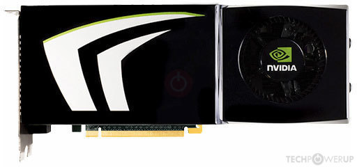
The GeForce GTX 260 Core 216 was a performance-segment graphics card by NVIDIA, launched on September 16th, 2008. Built on the 65 nm process, and based on the GT200 graphics processor, in its G200-103-A2 variant, the card supports DirectX 11.1. Even though it supports DirectX 11, the feature level is only 10_0, which can be problematic with many DirectX 11 & DirectX 12 titles. The GT200 graphics processor is a large chip with a die area of 576 mm² and 1,400 million transistors. Unlike the fully unlocked GeForce GTX 280, which uses the same GPU but has all 240 shaders enabled, NVIDIA has disabled some shading units on the GeForce GTX 260 Core 216 to reach the product's target shader count. It features 216 shading units, 72 texture mapping units, and 28 ROPs. NVIDIA has paired 896 MB GDDR3 memory with the GeForce GTX 260 Core 216, which are connected using a 448-bit memory interface. The GPU is operating at a frequency of 576 MHz, memory is running at 999 MHz.
Being a dual-slot card, the NVIDIA GeForce GTX 260 Core 216 draws power from 2x 6-pin power connectors, with power draw rated at 182 W maximum. Display outputs include: 2x DVI, 1x S-Video. GeForce GTX 260 Core 216 is connected to the rest of the system using a PCI-Express 2.0 x16 interface. The card measures 267 mm in length, and features a dual-slot cooling solution. Its price at launch was 299 US Dollars.
Being a dual-slot card, the NVIDIA GeForce GTX 260 Core 216 draws power from 2x 6-pin power connectors, with power draw rated at 182 W maximum. Display outputs include: 2x DVI, 1x S-Video. GeForce GTX 260 Core 216 is connected to the rest of the system using a PCI-Express 2.0 x16 interface. The card measures 267 mm in length, and features a dual-slot cooling solution. Its price at launch was 299 US Dollars.
Graphics Processor
Graphics Card
- Release Date
- Sep 16th, 2008
- Generation
- GeForce 200
- Predecessor
- GeForce 9
- Successor
- GeForce 400
- Production
- End-of-life
- Launch Price
- 299 USD
- Bus Interface
- PCIe 2.0 x16
- Reviews
- 137 in our database
Relative Performance
Based on TPU review data: "Performance Summary" at 1920x1080, 4K for 2080 Ti and faster.
Performance estimated based on architecture, shader count and clocks.
Clock Speeds
- GPU Clock
- 576 MHz
- Shader Clock
- 1242 MHz
- Memory Clock
-
999 MHz
1998 Mbps effective
Memory
- Memory Size
- 896 MB
- Memory Type
- GDDR3
- Memory Bus
- 448 bit
- Bandwidth
- 111.9 GB/s
Render Config
- Shading Units
- 216
- TMUs
- 72
- ROPs
- 28
- SM Count
- 27
- L2 Cache
- 224 KB
Theoretical Performance
- Pixel Rate
- 16.13 GPixel/s
- Texture Rate
- 41.47 GTexel/s
- FP32 (float)
- 536.5 GFLOPS
- FP64 (double)
- 67.07 GFLOPS (1:8)
Board Design
- Slot Width
- Dual-slot
- Length
- 267 mm
10.5 inches
- TDP
- 182 W
- Suggested PSU
- 450 W
- Outputs
- 2x DVI
1x S-Video
- Power Connectors
- 2x 6-pin
- Board Number
- P651 SKU 4,
P651 SKU 9,
P654 SKU 51
Graphics Features
- DirectX
- 11.1 (10_0)
- OpenGL
- 3.3
- OpenCL
- 1.1
- Vulkan
- N/A
- CUDA
- 1.3
- Shader Model
- 4.0
GT200 GPU Notes
| PureVideo HD: VP2 VDPAU: Feature Set A |
Retail boards based on this design (6)
| Name | GPU Clock | Memory Clock | Other Changes |
|---|---|---|---|
| 576 MHz | 999 MHz | ||
| 576 MHz | 999 MHz | 1792 MB | |
| 670 MHz | 1152 MHz | ||
| 648 MHz | 1053 MHz | ||
| 648 MHz | 1053 MHz | ||
| 626 MHz | 1053 MHz |


Apr 19th, 2024 20:51 EDT
change timezone
Latest GPU Drivers
New Forum Posts
- I just succesfully baked DDR4 (70)
- Windows 11 General Discussion (5014)
- GTX 1060 6GB ASUS GPU Shuts Down after 5min of Gaming (4)
- Official Board Game Discussion (1)
- USB C to USB A hub (42)
- The Official Linux/Unix Desktop Screenshots Megathread (688)
- AMD RX 7000 series GPU Owners' Club (1068)
- I9 13890HX undervolting Suggestions (4)
- Undervolting Dell XPS 14 9440 is it possible? (7)
- Share your AIDA 64 cache and memory benchmark here (2884)
Popular Reviews
- Horizon Forbidden West Performance Benchmark Review - 30 GPUs Tested
- Fractal Design Terra Review
- Corsair 2000D Airflow Review
- Thermalright Phantom Spirit 120 EVO Review
- Minisforum EliteMini UM780 XTX (AMD Ryzen 7 7840HS) Review
- Creative Pebble X Plus Review
- FiiO KB3 HiFi Mechanical Keyboard Review - Integrated DAC/Amp!
- ASUS GeForce RTX 4090 STRIX OC Review
- NVIDIA GeForce RTX 4090 Founders Edition Review - Impressive Performance
- ASUS GeForce RTX 4090 Matrix Platinum Review - The RTX 4090 Ti
Controversial News Posts
- Sony PlayStation 5 Pro Specifications Confirmed, Console Arrives Before Holidays (111)
- NVIDIA Points Intel Raptor Lake CPU Users to Get Help from Intel Amid System Instability Issues (102)
- US Government Wants Nuclear Plants to Offload AI Data Center Expansion (98)
- AMD "Strix Halo" Zen 5 Mobile Processor Pictured: Chiplet-based, Uses 256-bit LPDDR5X (84)
- Windows 10 Security Updates to Cost $61 After 2025, $427 by 2028 (82)
- Developers of Outpost Infinity Siege Recommend Underclocking i9-13900K and i9-14900K for Stability on Machines with RTX 4090 (82)
- TechPowerUp Hiring: Reviewers Wanted for Motherboards, Laptops, Gaming Handhelds and Prebuilt Desktops (72)
- Intel Realizes the Only Way to Save x86 is to Democratize it, Reopens x86 IP Licensing (70)