Report an Error


AMD Radeon R7 240
- Graphics Processor
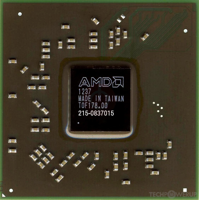
- Oland
- Cores
- 320
- TMUs
- 20
- ROPs
- 8
- Memory Size
- 2 GB
- Memory Type
- DDR3
- Bus Width
- 128 bit
GPU
Recommended Gaming Resolutions:
- 1366x768
- 1600x900
- 1920x1080
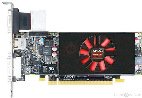
The Radeon R7 240 was an entry-level graphics card by AMD, launched on October 8th, 2013. Built on the 28 nm process, and based on the Oland graphics processor, in its Oland PRO variant, the card supports DirectX 12. Even though it supports DirectX 12, the feature level is only 11_1, which can be problematic with newer DirectX 12 titles. The Oland graphics processor is a relatively small chip with a die area of only 77 mm² and 950 million transistors. Unlike the fully unlocked Radeon HD 8670 OEM, which uses the same GPU but has all 384 shaders enabled, AMD has disabled some shading units on the Radeon R7 240 to reach the product's target shader count. It features 320 shading units, 20 texture mapping units, and 8 ROPs. AMD has paired 2,048 MB DDR3 memory with the Radeon R7 240, which are connected using a 128-bit memory interface. The GPU is operating at a frequency of 730 MHz, which can be boosted up to 780 MHz, memory is running at 900 MHz.
Being a single-slot card, the AMD Radeon R7 240 does not require any additional power connector, its power draw is rated at 30 W maximum. Display outputs include: 1x DVI, 1x HDMI 1.4a, 1x VGA. Radeon R7 240 is connected to the rest of the system using a PCI-Express 3.0 x8 interface. The card measures 168 mm in length, 69 mm in width, and features a single-slot cooling solution. Its price at launch was 69 US Dollars.
Being a single-slot card, the AMD Radeon R7 240 does not require any additional power connector, its power draw is rated at 30 W maximum. Display outputs include: 1x DVI, 1x HDMI 1.4a, 1x VGA. Radeon R7 240 is connected to the rest of the system using a PCI-Express 3.0 x8 interface. The card measures 168 mm in length, 69 mm in width, and features a single-slot cooling solution. Its price at launch was 69 US Dollars.
Graphics Processor
Graphics Card
- Release Date
- Oct 8th, 2013
- Generation
-
Volcanic Islands
(R7 200)
- Predecessor
- Sea Islands
- Successor
- Pirate Islands
- Production
- End-of-life
- Launch Price
- 69 USD
- Bus Interface
- PCIe 3.0 x8
- Reviews
- 5 in our database
Relative Performance
Based on TPU review data: "Performance Summary" at 1920x1080, 4K for 2080 Ti and faster.
Performance estimated based on architecture, shader count and clocks.
Clock Speeds
- Base Clock
- 730 MHz
- Boost Clock
- 780 MHz
- Memory Clock
-
900 MHz
1800 Mbps effective
Memory
- Memory Size
- 2 GB
- Memory Type
- DDR3
- Memory Bus
- 128 bit
- Bandwidth
- 28.80 GB/s
Render Config
- Shading Units
- 320
- TMUs
- 20
- ROPs
- 8
- Compute Units
- 5
- L1 Cache
- 16 KB (per CU)
- L2 Cache
- 256 KB
Theoretical Performance
- Pixel Rate
- 6.240 GPixel/s
- Texture Rate
- 15.60 GTexel/s
- FP32 (float)
- 499.2 GFLOPS
Board Design
- Slot Width
- Single-slot
- Length
- 168 mm
6.6 inches
- Width
- 69 mm
2.7 inches
- TDP
- 30 W
- Suggested PSU
- 200 W
- Outputs
- 1x DVI
1x HDMI 1.4a
1x VGA
- Power Connectors
- None
- Board Number
- C552,
C577
Graphics Features
- DirectX
- 12 (11_1)
- OpenGL
- 4.6
- OpenCL
- 2.1 (1.2)
- Vulkan
- 1.2.170
- Shader Model
- 6.5 (5.1)
Oland GPU Notes
| Generation: Sea Islands Mobile Variant: Mars / Opal / Litho Graphics/Compute: GFX6 (gfx601) Display Core Engine: 6.4 Unified Video Decoder: 4.0 Video Compression Engine: 1.0 CLRX: GCN 1.0 |
Retail boards based on this design (34)
| Name | GPU Clock | Boost Clock | Memory Clock | Other Changes |
|---|---|---|---|---|
| 730 MHz | 780 MHz | 1150 MHz | GDDR5, 147 mm/5.8 inches | |
| 730 MHz | 780 MHz | 900 MHz | 159 mm/6.3 inches | |
| 770 MHz | 820 MHz | 1150 MHz | 4 GB, GDDR5, 147 mm/5.8 inches | |
| 770 MHz | 820 MHz | 900 MHz | 4 GB, 159 mm/6.3 inches | |
| 600 MHz | 780 MHz | 800 MHz | 1024 MB, 147 mm/5.8 inches | |
| 730 MHz | 780 MHz | 900 MHz | 159 mm/6.3 inches | |
| 770 MHz | 820 MHz | 900 MHz | 4 GB, 159 mm/6.3 inches | |
| 730 MHz | 780 MHz | 900 MHz | 154 mm/6.1 inches | |
| 730 MHz | 780 MHz | 900 MHz | ||
| 780 MHz | 900 MHz | 800 MHz | 195 mm/7.7 inches | |
| 730 MHz | 780 MHz | 900 MHz | 199 mm/7.8 inches, Dual-slot | |
| 730 MHz | 780 MHz | 1150 MHz | 1024 MB, GDDR5, 172 mm/6.8 inches | |
| 730 MHz | 780 MHz | 900 MHz | 172 mm/6.8 inches | |
| 730 MHz | 780 MHz | 800 MHz | 167 mm/6.6 inches | |
| 730 MHz | 780 MHz | 1000 MHz | 1024 MB, GDDR5, Dual-slot | |
| 730 MHz | 780 MHz | 900 MHz | 208 mm/8.2 inches, Dual-slot | |
| 730 MHz | 780 MHz | 900 MHz | 144 mm/5.7 inches | |
| 730 MHz | 780 MHz | 900 MHz | 4 GB, 144 mm/5.7 inches | |
| 760 MHz | 810 MHz | 900 MHz | 208 mm/8.2 inches, Dual-slot | |
| 750 MHz | 800 MHz | 900 MHz | ||
| 730 MHz | 780 MHz | 900 MHz | 1024 MB, 145 mm/5.7 inches | |
| 730 MHz | 780 MHz | 1150 MHz | 1024 MB, GDDR5, 150 mm/5.9 inches | |
| 730 MHz | 780 MHz | 800 MHz | 145 mm/5.7 inches | |
| 730 MHz | 780 MHz | 900 MHz | 4 GB, 145 mm/5.7 inches | |
| 730 MHz | 780 MHz | 900 MHz | 169 mm/6.7 inches, 2x HDMI | |
| 730 MHz | 780 MHz | 1150 MHz | 1024 MB, GDDR5, 150 mm/5.9 inches | |
| 730 MHz | 780 MHz | 900 MHz | ||
| 750 MHz | 800 MHz | 900 MHz | ||
| 750 MHz | 800 MHz | 900 MHz | ||
| 730 MHz | 780 MHz | 800 MHz | 1024 MB, 175 mm/6.9 inches | |
| 730 MHz | 780 MHz | 800 MHz | 177 mm/7 inches, Dual-slot | |
| 730 MHz | 780 MHz | 800 MHz | 175 mm/6.9 inches | |
| 730 MHz | 780 MHz | 900 MHz | Dual-slot | |
| 730 MHz | 780 MHz | 900 MHz |


Apr 24th, 2024 17:10 EDT
change timezone
Latest GPU Drivers
New Forum Posts
- Best SSD for system drive (73)
- Meta Horizon OS (14)
- im new to throttelstop and i think i messed it up by copying others any hints would be very much aprreciated (0)
- Is It The 1080 TI The Best GPU Ever? (214)
- What phone you use as your daily driver? And, a discussion of them. (1470)
- Core PL1 + GPU PL1 + Ring EDP OTHER (6)
- Rare GPUs / Unreleased GPUs (1875)
- What's your latest tech purchase? (20336)
- What are you playing? (20524)
- Is there a way to have 2x chrome tabs side by side in fullscreen mode? (9)
Popular Reviews
- Fractal Design Terra Review
- Thermalright Phantom Spirit 120 EVO Review
- Corsair 2000D Airflow Review
- Minisforum EliteMini UM780 XTX (AMD Ryzen 7 7840HS) Review
- ASUS GeForce RTX 4090 STRIX OC Review
- NVIDIA GeForce RTX 4090 Founders Edition Review - Impressive Performance
- ASUS GeForce RTX 4090 Matrix Platinum Review - The RTX 4090 Ti
- MSI GeForce RTX 4090 Gaming X Trio Review
- MSI GeForce RTX 4090 Suprim X Review
- Gigabyte GeForce RTX 4090 Gaming OC Review
Controversial News Posts
- Sony PlayStation 5 Pro Specifications Confirmed, Console Arrives Before Holidays (116)
- NVIDIA Points Intel Raptor Lake CPU Users to Get Help from Intel Amid System Instability Issues (106)
- AMD "Strix Halo" Zen 5 Mobile Processor Pictured: Chiplet-based, Uses 256-bit LPDDR5X (101)
- US Government Wants Nuclear Plants to Offload AI Data Center Expansion (98)
- Windows 10 Security Updates to Cost $61 After 2025, $427 by 2028 (84)
- Developers of Outpost Infinity Siege Recommend Underclocking i9-13900K and i9-14900K for Stability on Machines with RTX 4090 (84)
- TechPowerUp Hiring: Reviewers Wanted for Motherboards, Laptops, Gaming Handhelds and Prebuilt Desktops (78)
- Intel Realizes the Only Way to Save x86 is to Democratize it, Reopens x86 IP Licensing (70)