Report an Error


NVIDIA Quadro K420
- Graphics Processor
- GK107
- Cores
- 192
- TMUs
- 16
- ROPs
- 16
- Memory Size
- 1024 MB
- Memory Type
- DDR3
- Bus Width
- 128 bit
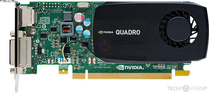

GPU

I/O
Bottom
Recommended Gaming Resolutions:
- 640x480
- 1280x720
- 1366x768
The Quadro K420 was a professional graphics card by NVIDIA, launched on July 22nd, 2014. Built on the 28 nm process, and based on the GK107 graphics processor, in its GK107-301-A2 variant, the card supports DirectX 12. The GK107 graphics processor is an average sized chip with a die area of 118 mm² and 1,270 million transistors. Unlike the fully unlocked GeForce GT 640 OEM, which uses the same GPU but has all 384 shaders enabled, NVIDIA has disabled some shading units on the Quadro K420 to reach the product's target shader count. It features 192 shading units, 16 texture mapping units, and 16 ROPs. NVIDIA has paired 1,024 MB DDR3 memory with the Quadro K420, which are connected using a 128-bit memory interface. The GPU is operating at a frequency of 876 MHz, memory is running at 891 MHz.
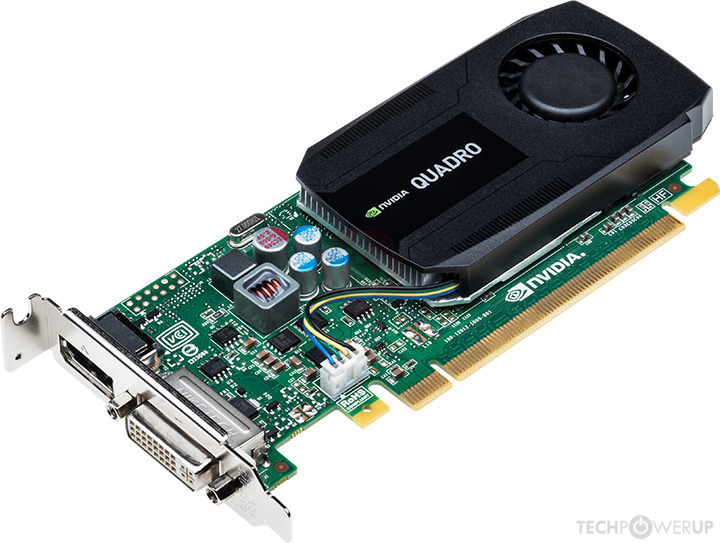
Being a single-slot card, the NVIDIA Quadro K420 does not require any additional power connector, its power draw is rated at 41 W maximum. Display outputs include: 1x DVI, 1x DisplayPort 1.2. Quadro K420 is connected to the rest of the system using a PCI-Express 2.0 x16 interface. The card measures 160 mm in length, 69 mm in width, and features a single-slot cooling solution.
Being a single-slot card, the NVIDIA Quadro K420 does not require any additional power connector, its power draw is rated at 41 W maximum. Display outputs include: 1x DVI, 1x DisplayPort 1.2. Quadro K420 is connected to the rest of the system using a PCI-Express 2.0 x16 interface. The card measures 160 mm in length, 69 mm in width, and features a single-slot cooling solution.
Graphics Processor
Graphics Card
- Release Date
- Jul 22nd, 2014
- Generation
-
Quadro Kepler
(Kx200)
- Predecessor
- Quadro Fermi
- Successor
- Quadro Maxwell
- Production
- End-of-life
- Bus Interface
- PCIe 2.0 x16
- Reviews
- 26 in our database
Relative Performance
Based on TPU review data: "Performance Summary" at 1920x1080, 4K for 2080 Ti and faster.
Performance estimated based on architecture, shader count and clocks.
Clock Speeds
- GPU Clock
- 876 MHz
- Memory Clock
-
891 MHz
1782 Mbps effective
Memory
- Memory Size
- 1024 MB
- Memory Type
- DDR3
- Memory Bus
- 128 bit
- Bandwidth
- 28.51 GB/s
Render Config
- Shading Units
- 192
- TMUs
- 16
- ROPs
- 16
- SMX Count
- 1
- L1 Cache
- 16 KB (per SMX)
- L2 Cache
- 256 KB
Theoretical Performance
- Pixel Rate
- 3.504 GPixel/s
- Texture Rate
- 14.02 GTexel/s
- FP32 (float)
- 336.4 GFLOPS
- FP64 (double)
- 14.02 GFLOPS (1:24)
Board Design
- Slot Width
- Single-slot
- Length
- 160 mm
6.3 inches
- Width
- 69 mm
2.7 inches
- TDP
- 41 W
- Suggested PSU
- 200 W
- Outputs
- 1x DVI
1x DisplayPort 1.2
- Power Connectors
- None
- Board Number
- P2012 SKU 506
Graphics Features
- DirectX
- 12 (11_0)
- OpenGL
- 4.6
- OpenCL
- 3.0
- Vulkan
- 1.2.175
- CUDA
- 3.0
- Shader Model
- 6.5 (5.1)
Card Notes
| Memory Variant: 2 GB |
GK107 GPU Notes
| NVENC: 1st Gen NVDEC: 1st Gen PureVideo HD: VP5 VDPAU: Feature Set D L1 Cache is configurable from 16 KB up to 48 KB per SMX |
Apr 17th, 2024 23:59 EDT
change timezone
Latest GPU Drivers
New Forum Posts
- 4K Gamers, How much VRAM do you have? (131)
- Your PC ATM (34483)
- Free Games Thread (3765)
- FINAL FANTASY XIV: Dawntrail Official Benchmark (46)
- EDP other basically constantly red while playing games (0)
- DDR5 RAM Speeds and the future (23)
- Will a RTX 4070 TI super bottleneck a Ryzen 9 7950X3D? (27)
- Looking for a great value 1080p gaming display (27)
- Gigabyte gpu model differences? (27)
- Why do i have such a huge Thread(?) usage imbalance (7)
Popular Reviews
- Horizon Forbidden West Performance Benchmark Review - 30 GPUs Tested
- PowerColor Radeon RX 7900 GRE Hellhound Review
- ASUS GeForce RTX 4090 Matrix Platinum Review - The RTX 4090 Ti
- Fractal Design Terra Review
- Corsair 2000D Airflow Review
- Minisforum EliteMini UM780 XTX (AMD Ryzen 7 7840HS) Review
- Creative Pebble X Plus Review
- FiiO KB3 HiFi Mechanical Keyboard Review - Integrated DAC/Amp!
- ASUS GeForce RTX 4090 STRIX OC Review
- NVIDIA GeForce RTX 4090 Founders Edition Review - Impressive Performance
Controversial News Posts
- Sony PlayStation 5 Pro Specifications Confirmed, Console Arrives Before Holidays (105)
- NVIDIA Points Intel Raptor Lake CPU Users to Get Help from Intel Amid System Instability Issues (102)
- US Government Wants Nuclear Plants to Offload AI Data Center Expansion (98)
- Windows 10 Security Updates to Cost $61 After 2025, $427 by 2028 (82)
- Developers of Outpost Infinity Siege Recommend Underclocking i9-13900K and i9-14900K for Stability on Machines with RTX 4090 (82)
- TechPowerUp Hiring: Reviewers Wanted for Motherboards, Laptops, Gaming Handhelds and Prebuilt Desktops (70)
- Intel Realizes the Only Way to Save x86 is to Democratize it, Reopens x86 IP Licensing (70)
- AMD Zen 5 Execution Engine Leaked, Features True 512-bit FPU (63)