Report an Error


AMD FirePro W2100
- Graphics Processor
- Oland
- Cores
- 320
- TMUs
- 20
- ROPs
- 8
- Memory Size
- 2 GB
- Memory Type
- DDR3
- Bus Width
- 128 bit

GPU
I/O

Rear

Back
Recommended Gaming Resolutions:
- 1280x720
- 1366x768
- 1600x900
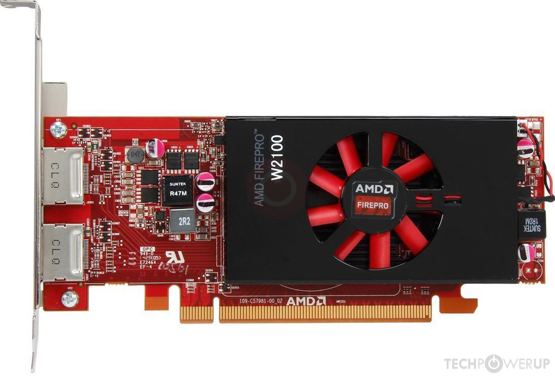
The FirePro W2100 was a professional graphics card by AMD, launched on August 12th, 2014. Built on the 28 nm process, and based on the Oland graphics processor, the card supports DirectX 12. The Oland graphics processor is a relatively small chip with a die area of only 77 mm² and 950 million transistors. Unlike the fully unlocked Radeon HD 8670 OEM, which uses the same GPU but has all 384 shaders enabled, AMD has disabled some shading units on the FirePro W2100 to reach the product's target shader count. It features 320 shading units, 20 texture mapping units, and 8 ROPs. AMD has paired 2,048 MB DDR3 memory with the FirePro W2100, which are connected using a 128-bit memory interface. The GPU is operating at a frequency of 630 MHz, which can be boosted up to 680 MHz, memory is running at 900 MHz.
Being a single-slot card, the AMD FirePro W2100 does not require any additional power connector, its power draw is rated at 26 W maximum. Display outputs include: 2x DisplayPort 1.2. FirePro W2100 is connected to the rest of the system using a PCI-Express 3.0 x8 interface. The card measures 168 mm in length, 69 mm in width, and features a single-slot cooling solution.
Being a single-slot card, the AMD FirePro W2100 does not require any additional power connector, its power draw is rated at 26 W maximum. Display outputs include: 2x DisplayPort 1.2. FirePro W2100 is connected to the rest of the system using a PCI-Express 3.0 x8 interface. The card measures 168 mm in length, 69 mm in width, and features a single-slot cooling solution.
Graphics Processor
Graphics Card
- Release Date
- Aug 12th, 2014
- Generation
-
FirePro GCN
(Wx100)
- Predecessor
- FirePro Terascale
- Successor
- Radeon Pro Polaris
- Production
- End-of-life
- Bus Interface
- PCIe 3.0 x8
Relative Performance
Based on TPU review data: "Performance Summary" at 1920x1080, 4K for 2080 Ti and faster.
Performance estimated based on architecture, shader count and clocks.
Clock Speeds
- Base Clock
- 630 MHz
- Boost Clock
- 680 MHz
- Memory Clock
-
900 MHz
1800 Mbps effective
Memory
- Memory Size
- 2 GB
- Memory Type
- DDR3
- Memory Bus
- 128 bit
- Bandwidth
- 28.80 GB/s
Render Config
- Shading Units
- 320
- TMUs
- 20
- ROPs
- 8
- Compute Units
- 5
- L1 Cache
- 16 KB (per CU)
- L2 Cache
- 256 KB
Theoretical Performance
- Pixel Rate
- 5.440 GPixel/s
- Texture Rate
- 13.60 GTexel/s
- FP32 (float)
- 435.2 GFLOPS
- FP64 (double)
- 27.20 GFLOPS (1:16)
Board Design
- Slot Width
- Single-slot
- Length
- 168 mm
6.6 inches
- Width
- 69 mm
2.7 inches
- TDP
- 26 W
- Suggested PSU
- 200 W
- Outputs
- 2x DisplayPort 1.2
- Power Connectors
- None
- Board Number
- 109-C57981-00_02
Graphics Features
- DirectX
- 12 (11_1)
- OpenGL
- 4.6
- OpenCL
- 2.1 (1.2)
- Vulkan
- 1.2.170
- Shader Model
- 6.5 (5.1)
Oland GPU Notes
| Generation: Sea Islands Mobile Variant: Mars / Opal / Litho Graphics/Compute: GFX6 (gfx601) Display Core Engine: 6.4 Unified Video Decoder: 4.0 Video Compression Engine: 1.0 CLRX: GCN 1.0 |
Retail boards based on this design (3)
| Name | GPU Clock | Boost Clock | Memory Clock | Other Changes |
|---|---|---|---|---|
| 630 MHz | 680 MHz | 900 MHz | ||
| 630 MHz | 680 MHz | 900 MHz | ||
| 630 MHz | 680 MHz | 900 MHz |


Apr 25th, 2024 07:49 EDT
change timezone
Latest GPU Drivers
New Forum Posts
- Bizarre Throttlestop issue (6)
- (Anti) SFF fun house (353)
- Core i5-6300U (17)
- Last game you purchased? (255)
- Share your AIDA 64 cache and memory benchmark here (2916)
- What phone you use as your daily driver? And, a discussion of them. (1472)
- What's your latest tech purchase? (20338)
- Meta Horizon OS (16)
- Alphacool CORE 1 CPU block - bulging with danger of splitting? (4)
- The TPU UK Clubhouse (24786)
Popular Reviews
- Fractal Design Terra Review
- Thermalright Phantom Spirit 120 EVO Review
- Corsair 2000D Airflow Review
- Minisforum EliteMini UM780 XTX (AMD Ryzen 7 7840HS) Review
- ASUS GeForce RTX 4090 STRIX OC Review
- NVIDIA GeForce RTX 4090 Founders Edition Review - Impressive Performance
- ASUS GeForce RTX 4090 Matrix Platinum Review - The RTX 4090 Ti
- MSI GeForce RTX 4090 Suprim X Review
- MSI GeForce RTX 4090 Gaming X Trio Review
- Gigabyte GeForce RTX 4090 Gaming OC Review
Controversial News Posts
- Sony PlayStation 5 Pro Specifications Confirmed, Console Arrives Before Holidays (116)
- NVIDIA Points Intel Raptor Lake CPU Users to Get Help from Intel Amid System Instability Issues (106)
- AMD "Strix Halo" Zen 5 Mobile Processor Pictured: Chiplet-based, Uses 256-bit LPDDR5X (101)
- US Government Wants Nuclear Plants to Offload AI Data Center Expansion (98)
- Windows 11 Now Officially Adware as Microsoft Embeds Ads in the Start Menu (86)
- Windows 10 Security Updates to Cost $61 After 2025, $427 by 2028 (84)
- Developers of Outpost Infinity Siege Recommend Underclocking i9-13900K and i9-14900K for Stability on Machines with RTX 4090 (84)
- AMD's RDNA 4 GPUs Could Stick with 18 Gbps GDDR6 Memory (80)