Report an Error


AMD Radeon R9 390X
- Graphics Processor
- Grenada
- Cores
- 2816
- TMUs
- 176
- ROPs
- 64
- Memory Size
- 8 GB
- Memory Type
- GDDR5
- Bus Width
- 512 bit

GPU

I/O

Top
Recommended Gaming Resolutions:
- 1920x1080
- 2560x1440
- 3840x2160
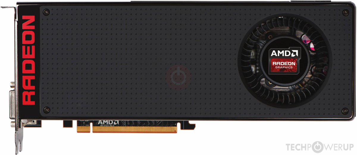
The Radeon R9 390X was a high-end graphics card by AMD, launched on June 18th, 2015. Built on the 28 nm process, and based on the Grenada graphics processor, in its Grenada XT variant, the card supports DirectX 12. This ensures that all modern games will run on Radeon R9 390X. The Grenada graphics processor is a large chip with a die area of 438 mm² and 6,200 million transistors. It features 2816 shading units, 176 texture mapping units, and 64 ROPs. AMD has paired 8 GB GDDR5 memory with the Radeon R9 390X, which are connected using a 512-bit memory interface. The GPU is operating at a frequency of 1050 MHz, memory is running at 1500 MHz (6 Gbps effective).
Being a dual-slot card, the AMD Radeon R9 390X draws power from 1x 6-pin + 1x 8-pin power connector, with power draw rated at 275 W maximum. Display outputs include: 2x DVI, 1x HDMI 1.4a, 1x DisplayPort 1.2. Radeon R9 390X is connected to the rest of the system using a PCI-Express 3.0 x16 interface. The card's dimensions are 275 mm x 109 mm x 36 mm, and it features a dual-slot cooling solution. Its price at launch was 429 US Dollars.
Being a dual-slot card, the AMD Radeon R9 390X draws power from 1x 6-pin + 1x 8-pin power connector, with power draw rated at 275 W maximum. Display outputs include: 2x DVI, 1x HDMI 1.4a, 1x DisplayPort 1.2. Radeon R9 390X is connected to the rest of the system using a PCI-Express 3.0 x16 interface. The card's dimensions are 275 mm x 109 mm x 36 mm, and it features a dual-slot cooling solution. Its price at launch was 429 US Dollars.
Graphics Processor
Graphics Card
- Release Date
- Jun 18th, 2015
- Generation
-
Pirate Islands
(R9 300)
- Predecessor
- Volcanic Islands
- Successor
- Arctic Islands
- Production
- End-of-life
- Launch Price
- 429 USD
- Bus Interface
- PCIe 3.0 x16
- Reviews
- 60 in our database
Relative Performance
Based on TPU review data: "Performance Summary" at 1920x1080, 4K for 2080 Ti and faster.
Clock Speeds
- GPU Clock
- 1050 MHz
- Memory Clock
-
1500 MHz
6 Gbps effective
Memory
- Memory Size
- 8 GB
- Memory Type
- GDDR5
- Memory Bus
- 512 bit
- Bandwidth
- 384.0 GB/s
Render Config
- Shading Units
- 2816
- TMUs
- 176
- ROPs
- 64
- Compute Units
- 44
- L1 Cache
- 16 KB (per CU)
- L2 Cache
- 1024 KB
Theoretical Performance
- Pixel Rate
- 67.20 GPixel/s
- Texture Rate
- 184.8 GTexel/s
- FP32 (float)
- 5.914 TFLOPS
- FP64 (double)
- 739.2 GFLOPS (1:8)
Board Design
- Slot Width
- Dual-slot
- Length
- 275 mm
10.8 inches
- Width
- 109 mm
4.3 inches
- Height
- 36 mm
1.4 inches
- TDP
- 275 W
- Suggested PSU
- 600 W
- Outputs
- 2x DVI
1x HDMI 1.4a
1x DisplayPort 1.2
- Power Connectors
- 1x 6-pin + 1x 8-pin
- Board Number
- 109-C67157-00_02,
C679-37
Graphics Features
- DirectX
- 12 (12_0)
- OpenGL
- 4.6
- OpenCL
- 2.1
- Vulkan
- 1.2.170
- Shader Model
- 6.5
Grenada GPU Notes
| Generation: Volcanic Islands Desktop Variant: Hawaii / Vesuvius Graphics/Compute: GFX7 (gfx702) Display Core Engine: 8.5 Unified Video Decoder: 4.2 Video Compression Engine: 2.0 System DMA: 1.0.0 CLRX: GCN 1.1.0 |
Retail boards based on this design (17)
| Name | GPU Clock | Memory Clock | Other Changes |
|---|---|---|---|
| 1050 MHz | 1500 MHz | 252 mm/9.9 inches | |
| 1050 MHz | 1500 MHz | 287 mm/11.3 inches | |
| 1070 MHz | 1500 MHz | 300 mm/11.8 inches | |
| 1060 MHz | 1500 MHz | 305 mm/12 inches | |
| 1060 MHz | 1500 MHz | 243 mm/9.6 inches, 1x DVI 1x HDMI 3x DisplayPort | |
| 1050 MHz | 1500 MHz | 243 mm/9.6 inches, 1x DVI 1x HDMI 3x DisplayPort | |
| 1050 MHz | 1500 MHz | 297 mm/11.7 inches | |
| 1060 MHz | 1500 MHz | 297 mm/11.7 inches | |
| 1070 MHz | 1500 MHz | 297 mm/11.7 inches | |
| 1080 MHz | 1525 MHz | 277 mm/10.9 inches | |
| 1100 MHz | 1525 MHz | 285 mm/11.2 inches | |
| 1060 MHz | 1500 MHz | 305 mm/12 inches | |
| 1060 MHz | 1500 MHz | 307 mm/12.1 inches, 1x DVI 1x HDMI 3x DisplayPort | |
| 1055 MHz | 1500 MHz | 308 mm/12.1 inches, 1x DVI 1x HDMI 3x DisplayPort | |
| 1080 MHz | 1500 MHz | 307 mm/12.1 inches, 1x DVI 1x HDMI 3x DisplayPort | |
| 1050 MHz | 1500 MHz | 295 mm/11.6 inches | |
| 1090 MHz | 1500 MHz | 295 mm/11.6 inches |


Apr 24th, 2024 06:07 EDT
change timezone
Latest GPU Drivers
New Forum Posts
- Windows 11 General Discussion (5021)
- What's your latest tech purchase? (20331)
- My computer setup - Request for opinions (13)
- Share your AIDA 64 cache and memory benchmark here (2914)
- EK seems to be having major issues (28)
- CYBERPUNK 2077 O.F. (5)
- The TPU UK Clubhouse (24776)
- What phone you use as your daily driver? And, a discussion of them. (1458)
- Which new games will you be buying? (309)
- Official Board Game Discussion (15)
Popular Reviews
- Fractal Design Terra Review
- Corsair 2000D Airflow Review
- Thermalright Phantom Spirit 120 EVO Review
- Minisforum EliteMini UM780 XTX (AMD Ryzen 7 7840HS) Review
- ASUS GeForce RTX 4090 STRIX OC Review
- NVIDIA GeForce RTX 4090 Founders Edition Review - Impressive Performance
- ASUS GeForce RTX 4090 Matrix Platinum Review - The RTX 4090 Ti
- MSI GeForce RTX 4090 Suprim X Review
- MSI GeForce RTX 4090 Gaming X Trio Review
- Gigabyte GeForce RTX 4090 Gaming OC Review
Controversial News Posts
- Sony PlayStation 5 Pro Specifications Confirmed, Console Arrives Before Holidays (116)
- NVIDIA Points Intel Raptor Lake CPU Users to Get Help from Intel Amid System Instability Issues (106)
- AMD "Strix Halo" Zen 5 Mobile Processor Pictured: Chiplet-based, Uses 256-bit LPDDR5X (101)
- US Government Wants Nuclear Plants to Offload AI Data Center Expansion (98)
- Windows 10 Security Updates to Cost $61 After 2025, $427 by 2028 (84)
- Developers of Outpost Infinity Siege Recommend Underclocking i9-13900K and i9-14900K for Stability on Machines with RTX 4090 (84)
- TechPowerUp Hiring: Reviewers Wanted for Motherboards, Laptops, Gaming Handhelds and Prebuilt Desktops (77)
- Intel Realizes the Only Way to Save x86 is to Democratize it, Reopens x86 IP Licensing (70)