Report an Error


NVIDIA GeForce GTX 570
- Graphics Processor
- GF110
- Cores
- 480
- TMUs
- 60
- ROPs
- 40
- Memory Size
- 1280 MB
- Memory Type
- GDDR5
- Bus Width
- 320 bit

GPU

I/O

Top

Bottom

PCB Front

PCB Back
Recommended Gaming Resolutions:
- 1600x900
- 1920x1080
- 2560x1440
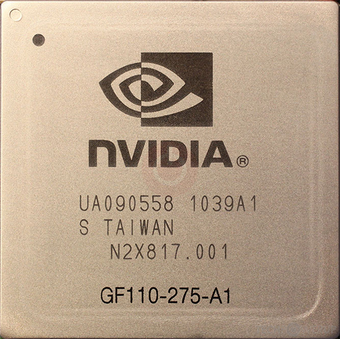
The GeForce GTX 570 was a performance-segment graphics card by NVIDIA, launched on December 7th, 2010. Built on the 40 nm process, and based on the GF110 graphics processor, in its GF110-275-A1 variant, the card supports DirectX 12. Even though it supports DirectX 12, the feature level is only 11_0, which can be problematic with newer DirectX 12 titles. The GF110 graphics processor is a large chip with a die area of 520 mm² and 3,000 million transistors. Unlike the fully unlocked GeForce GTX 580, which uses the same GPU but has all 512 shaders enabled, NVIDIA has disabled some shading units on the GeForce GTX 570 to reach the product's target shader count. It features 480 shading units, 60 texture mapping units, and 40 ROPs. NVIDIA has paired 1,280 MB GDDR5 memory with the GeForce GTX 570, which are connected using a 320-bit memory interface. The GPU is operating at a frequency of 732 MHz, memory is running at 950 MHz (3.8 Gbps effective).
Being a dual-slot card, the NVIDIA GeForce GTX 570 draws power from 2x 6-pin power connectors, with power draw rated at 219 W maximum. Display outputs include: 2x DVI, 1x mini-HDMI 1.3a. GeForce GTX 570 is connected to the rest of the system using a PCI-Express 2.0 x16 interface. The card measures 267 mm in length, and features a dual-slot cooling solution. Its price at launch was 349 US Dollars.
Being a dual-slot card, the NVIDIA GeForce GTX 570 draws power from 2x 6-pin power connectors, with power draw rated at 219 W maximum. Display outputs include: 2x DVI, 1x mini-HDMI 1.3a. GeForce GTX 570 is connected to the rest of the system using a PCI-Express 2.0 x16 interface. The card measures 267 mm in length, and features a dual-slot cooling solution. Its price at launch was 349 US Dollars.
Graphics Processor
Graphics Card
- Release Date
- Dec 7th, 2010
- Generation
- GeForce 500
- Predecessor
- GeForce 400
- Successor
- GeForce 600
- Production
- End-of-life
- Launch Price
- 349 USD
- Bus Interface
- PCIe 2.0 x16
- Reviews
- 76 in our database
Relative Performance
Based on TPU review data: "Performance Summary" at 1920x1080, 4K for 2080 Ti and faster.
Clock Speeds
- GPU Clock
- 732 MHz
- Shader Clock
- 1464 MHz
- Memory Clock
-
950 MHz
3.8 Gbps effective
Memory
- Memory Size
- 1280 MB
- Memory Type
- GDDR5
- Memory Bus
- 320 bit
- Bandwidth
- 152.0 GB/s
Render Config
- Shading Units
- 480
- TMUs
- 60
- ROPs
- 40
- SM Count
- 15
- L1 Cache
- 64 KB (per SM)
- L2 Cache
- 640 KB
Theoretical Performance
- Pixel Rate
- 21.96 GPixel/s
- Texture Rate
- 43.92 GTexel/s
- FP32 (float)
- 1,405 GFLOPS
- FP64 (double)
- 175.7 GFLOPS (1:8)
Board Design
- Slot Width
- Dual-slot
- Length
- 267 mm
10.5 inches
- TDP
- 219 W
- Suggested PSU
- 550 W
- Outputs
- 2x DVI
1x mini-HDMI 1.3a
- Power Connectors
- 2x 6-pin
- Board Number
- P1261 SKU 5
Graphics Features
- DirectX
- 12 (11_0)
- OpenGL
- 4.6
- OpenCL
- 1.1
- Vulkan
- N/A
- CUDA
- 2.0
- Shader Model
- 5.1
GF110 GPU Notes
| PureVideo HD: VP4 VDPAU: Feature Set C GF110 has 4 GPCs each capable of 8 pixels per clock. This limits complete GPU to 32 pixels per clock and because of that it can't feed all 48 ROPs when they all require data at the same time. Additional ROPs however can be used for MSAA (because it doesn't require additional data from rasterizers, while giving more work to ROPs.) The complete die contains 64 texture address units and 256 texture filtering units. |
Retail boards based on this design (15)
| Name | GPU Clock | Memory Clock | Other Changes |
|---|---|---|---|
| 732 MHz | 950 MHz | ||
| 797 MHz | 975 MHz | 2x DVI 1x HDMI 1x DisplayPort | |
| 750 MHz | 975 MHz | 228 mm/9 inches, 2x DVI 1x HDMI 1x DisplayPort | |
| 800 MHz | 1000 MHz | 228 mm/9 inches, 2x DVI 1x HDMI 1x DisplayPort | |
| 750 MHz | 975 MHz | 2x DVI 1x HDMI 1x DisplayPort | |
| 800 MHz | 950 MHz | 253 mm/10 inches, 4x DVI | |
| 780 MHz | 950 MHz | 282 mm/11.1 inches | |
| 800 MHz | 950 MHz | 253 mm/10 inches, 4x DVI | |
| 750 MHz | 975 MHz | 228 mm/9 inches, 2x DVI 1x HDMI 1x DisplayPort | |
| 800 MHz | 1000 MHz | 241 mm/9.5 inches, 2x DVI 1x HDMI 1x DisplayPort | |
| 772 MHz | 972 MHz | ||
| 810 MHz | 990 MHz | ||
| 772 MHz | 1053 MHz | 279 mm/11 inches | |
| 752 MHz | 1000 MHz | 279 mm/11 inches, Single-slot, 1x DVI 1x HDMI 1x DisplayPort | |
| 780 MHz | 1000 MHz |


Apr 24th, 2024 21:16 EDT
change timezone
Latest GPU Drivers
New Forum Posts
- Cinebench crashed my PC. My Wi-Fi stopped working, and I keep getting a "Please wait" screen when I boot up my PC. (30)
- The TPU UK Clubhouse (24783)
- (Anti) SFF fun house (346)
- Sharing experience with MSI RTX 3070 vBIOS update to enable Resizable Bar with MB Z490 (2)
- Share your AIDA 64 cache and memory benchmark here (2915)
- Will a RTX 4070 TI super bottleneck a Ryzen 9 7950X3D? (58)
- The best *budget* ATX PC case on the market? (24)
- GTX 1070 Ti - TDP Issues - Always Power Throttling (4)
- 2022-X58/1366 PIN Motherboards NVME M.2 SSD BIOS MOD Collection (656)
- Meta Horizon OS (15)
Popular Reviews
- Fractal Design Terra Review
- Thermalright Phantom Spirit 120 EVO Review
- Corsair 2000D Airflow Review
- Minisforum EliteMini UM780 XTX (AMD Ryzen 7 7840HS) Review
- ASUS GeForce RTX 4090 STRIX OC Review
- NVIDIA GeForce RTX 4090 Founders Edition Review - Impressive Performance
- ASUS GeForce RTX 4090 Matrix Platinum Review - The RTX 4090 Ti
- MSI GeForce RTX 4090 Suprim X Review
- MSI GeForce RTX 4090 Gaming X Trio Review
- Gigabyte GeForce RTX 4090 Gaming OC Review
Controversial News Posts
- Sony PlayStation 5 Pro Specifications Confirmed, Console Arrives Before Holidays (116)
- NVIDIA Points Intel Raptor Lake CPU Users to Get Help from Intel Amid System Instability Issues (106)
- AMD "Strix Halo" Zen 5 Mobile Processor Pictured: Chiplet-based, Uses 256-bit LPDDR5X (101)
- US Government Wants Nuclear Plants to Offload AI Data Center Expansion (98)
- Windows 10 Security Updates to Cost $61 After 2025, $427 by 2028 (84)
- Developers of Outpost Infinity Siege Recommend Underclocking i9-13900K and i9-14900K for Stability on Machines with RTX 4090 (84)
- TechPowerUp Hiring: Reviewers Wanted for Motherboards, Laptops, Gaming Handhelds and Prebuilt Desktops (78)
- AMD's RDNA 4 GPUs Could Stick with 18 Gbps GDDR6 Memory (73)