Report an Error


AMD Radeon R9 380
- Graphics Processor
- Antigua
- Cores
- 1792
- TMUs
- 112
- ROPs
- 32
- Memory Size
- 2 GB
- Memory Type
- GDDR5
- Bus Width
- 256 bit


GPU

Top
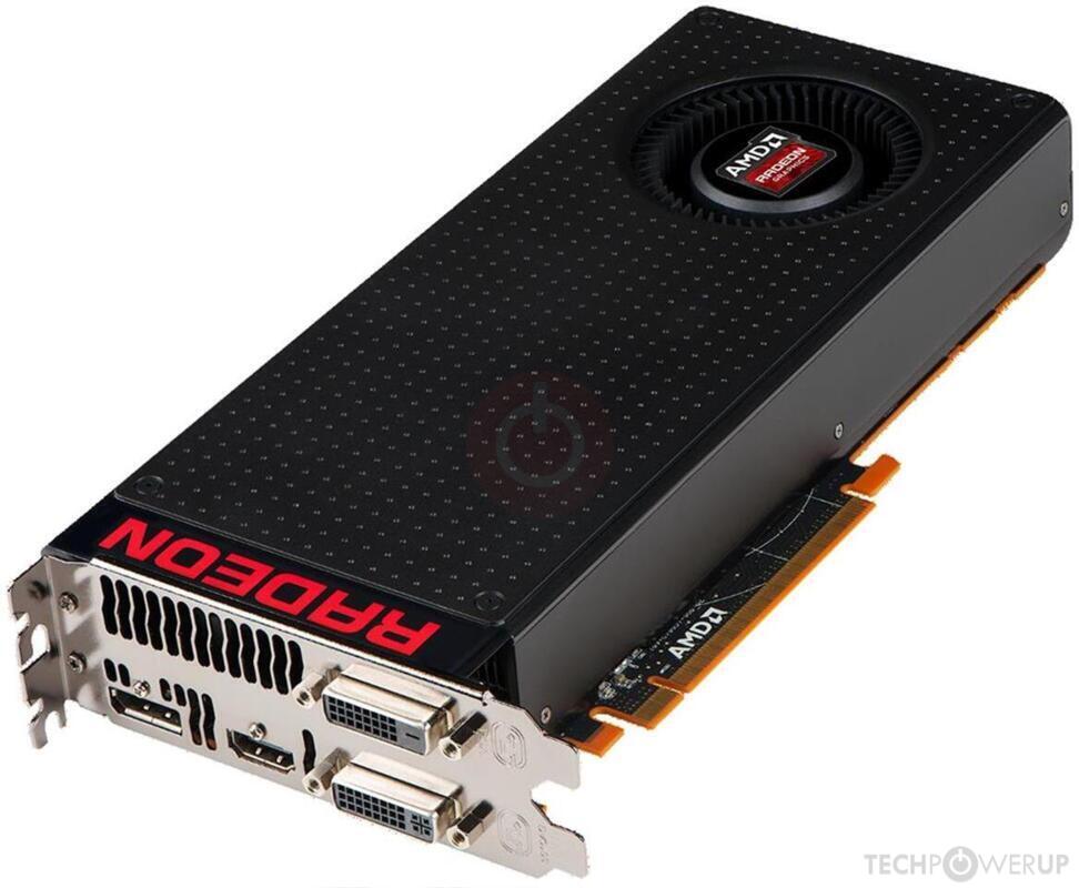
Bottom
Recommended Gaming Resolutions:
- 1600x900
- 1920x1080
- 2560x1440
The Radeon R9 380 was a performance-segment graphics card by AMD, launched on June 18th, 2015. Built on the 28 nm process, and based on the Antigua graphics processor, in its Antigua PRO variant, the card supports DirectX 12. This ensures that all modern games will run on Radeon R9 380. The Antigua graphics processor is a large chip with a die area of 366 mm² and 5,000 million transistors. Unlike the fully unlocked Radeon R9 380X, which uses the same GPU but has all 2048 shaders enabled, AMD has disabled some shading units on the Radeon R9 380 to reach the product's target shader count. It features 1792 shading units, 112 texture mapping units, and 32 ROPs. AMD has paired 2,048 MB GDDR5 memory with the Radeon R9 380, which are connected using a 256-bit memory interface. The GPU is operating at a frequency of 970 MHz, memory is running at 1375 MHz (5.5 Gbps effective).
Being a dual-slot card, the AMD Radeon R9 380 draws power from 2x 6-pin power connectors, with power draw rated at 190 W maximum. Display outputs include: 2x DVI, 1x HDMI 1.4a, 1x DisplayPort 1.2. Radeon R9 380 is connected to the rest of the system using a PCI-Express 3.0 x16 interface. The card measures 221 mm in length, 111 mm in width, and features a dual-slot cooling solution. Its price at launch was 199 US Dollars.
Being a dual-slot card, the AMD Radeon R9 380 draws power from 2x 6-pin power connectors, with power draw rated at 190 W maximum. Display outputs include: 2x DVI, 1x HDMI 1.4a, 1x DisplayPort 1.2. Radeon R9 380 is connected to the rest of the system using a PCI-Express 3.0 x16 interface. The card measures 221 mm in length, 111 mm in width, and features a dual-slot cooling solution. Its price at launch was 199 US Dollars.
Graphics Processor
Graphics Card
- Release Date
- Jun 18th, 2015
- Generation
-
Pirate Islands
(R9 300)
- Predecessor
- Volcanic Islands
- Successor
- Arctic Islands
- Production
- End-of-life
- Launch Price
- 199 USD
- Bus Interface
- PCIe 3.0 x16
- Reviews
- 39 in our database
Relative Performance
Based on TPU review data: "Performance Summary" at 1920x1080, 4K for 2080 Ti and faster.
Clock Speeds
- GPU Clock
- 970 MHz
- Memory Clock
-
1375 MHz
5.5 Gbps effective
Memory
- Memory Size
- 2 GB
- Memory Type
- GDDR5
- Memory Bus
- 256 bit
- Bandwidth
- 176.0 GB/s
Render Config
- Shading Units
- 1792
- TMUs
- 112
- ROPs
- 32
- Compute Units
- 28
- L1 Cache
- 16 KB (per CU)
- L2 Cache
- 512 KB
Theoretical Performance
- Pixel Rate
- 31.04 GPixel/s
- Texture Rate
- 108.6 GTexel/s
- FP16 (half)
- 3.476 TFLOPS (1:1)
- FP32 (float)
- 3.476 TFLOPS
- FP64 (double)
- 217.3 GFLOPS (1:16)
Board Design
- Slot Width
- Dual-slot
- Length
- 221 mm
8.7 inches
- Width
- 111 mm
4.4 inches
- TDP
- 190 W
- Suggested PSU
- 450 W
- Outputs
- 2x DVI
1x HDMI 1.4a
1x DisplayPort 1.2
- Power Connectors
- 2x 6-pin
- Board Number
- C766
Graphics Features
- DirectX
- 12 (12_0)
- OpenGL
- 4.6
- OpenCL
- 2.1
- Vulkan
- 1.2.170
- Shader Model
- 6.5
Antigua GPU Notes
| Generation: Volcanic Islands Desktop Variant: Tonga Mobile Variant: Amethyst Graphics/Compute: GFX8 (gfx802) Display Core Engine: 10.0 Unified Video Decoder: 5.0 Video Compression Engine: 3.0 System DMA: 3.0.0 CLRX: GCN 1.2.0 |
Retail boards based on this design (26)
| Name | GPU Clock | Memory Clock | Other Changes |
|---|---|---|---|
| 970 MHz | 1375 MHz | 273 mm/10.7 inches | |
| 970 MHz | 1375 MHz | 4 GB, 271 mm/10.7 inches | |
| 990 MHz | 1375 MHz | 273 mm/10.7 inches | |
| 990 MHz | 1375 MHz | 4 GB, 271 mm/10.7 inches | |
| 980 MHz | 1475 MHz | 4 GB, 207 mm/8.1 inches | |
| 990 MHz | 1425 MHz | 4 GB, 234 mm/9.2 inches | |
| 970 MHz | 1375 MHz | 263 mm/10.4 inches | |
| 970 MHz | 1375 MHz | 4 GB, 234 mm/9.2 inches | |
| 980 MHz | 1375 MHz | 263 mm/10.4 inches | |
| 990 MHz | 1375 MHz | 270 mm/10.6 inches | |
| 990 MHz | 1425 MHz | 4 GB, 270 mm/10.6 inches | |
| 980 MHz | 1375 MHz | 268 mm/10.6 inches | |
| 980 MHz | 1425 MHz | 4 GB, 268 mm/10.6 inches | |
| 980 MHz | 1375 MHz | 254 mm/10 inches | |
| 980 MHz | 1475 MHz | 4 GB, 207 mm/8.1 inches | |
| 918 MHz | 1425 MHz | 4 GB, 207 mm/8.1 inches | |
| 985 MHz | 1375 MHz | 263 mm/10.4 inches | |
| 1000 MHz | 1400 MHz | 236 mm/9.3 inches | |
| 985 MHz | 1450 MHz | 4 GB, 237 mm/9.3 inches | |
| 1010 MHz | 1450 MHz | 236 mm/9.3 inches | |
| 1010 MHz | 1450 MHz | 4 GB, 236 mm/9.3 inches | |
| 980 MHz | 1400 MHz | 170 mm/6.7 inches, 1x DVI 1x HDMI 2x mini-DisplayPort | |
| 1000 MHz | 1450 MHz | 4 GB, 170 mm/6.7 inches, 1x DVI 1x HDMI 2x mini-DisplayPort | |
| 990 MHz | 1375 MHz | 234 mm/9.2 inches | |
| 990 MHz | 1425 MHz | 4 GB, 234 mm/9.2 inches | |
| 1030 MHz | 1450 MHz | 234 mm/9.2 inches |


Apr 25th, 2024 12:03 EDT
change timezone
Latest GPU Drivers
New Forum Posts
- Have you got pie today? (16317)
- Milestones (13874)
- WCG Daily Numbers (12496)
- TPU's Rosetta Milestones and Daily Pie Thread (1859)
- ThrottleStop 9.6 Voltage won't change (4)
- Folding Pie and Milestones!! (9008)
- Making Audio Enhancers Work on Windows (2649)
- Random blue screen from winload.efi error (0xc000000e) (1)
- which new soundcard or which 4.1 speakers kits ? (10)
- Alphacool CORE 1 CPU block - bulging with danger of splitting? (8)
Popular Reviews
- Fractal Design Terra Review
- Thermalright Phantom Spirit 120 EVO Review
- Corsair 2000D Airflow Review
- Minisforum EliteMini UM780 XTX (AMD Ryzen 7 7840HS) Review
- ASUS GeForce RTX 4090 STRIX OC Review
- NVIDIA GeForce RTX 4090 Founders Edition Review - Impressive Performance
- ASUS GeForce RTX 4090 Matrix Platinum Review - The RTX 4090 Ti
- MSI GeForce RTX 4090 Suprim X Review
- MSI GeForce RTX 4090 Gaming X Trio Review
- Gigabyte GeForce RTX 4090 Gaming OC Review
Controversial News Posts
- Sony PlayStation 5 Pro Specifications Confirmed, Console Arrives Before Holidays (116)
- NVIDIA Points Intel Raptor Lake CPU Users to Get Help from Intel Amid System Instability Issues (106)
- AMD "Strix Halo" Zen 5 Mobile Processor Pictured: Chiplet-based, Uses 256-bit LPDDR5X (101)
- US Government Wants Nuclear Plants to Offload AI Data Center Expansion (98)
- Windows 11 Now Officially Adware as Microsoft Embeds Ads in the Start Menu (93)
- AMD's RDNA 4 GPUs Could Stick with 18 Gbps GDDR6 Memory (85)
- Developers of Outpost Infinity Siege Recommend Underclocking i9-13900K and i9-14900K for Stability on Machines with RTX 4090 (85)
- Windows 10 Security Updates to Cost $61 After 2025, $427 by 2028 (84)