Report an Error


AMD Radeon E6465
- Graphics Processor
- Caicos
- Cores
- 160
- TMUs
- 8
- ROPs
- 4
- Memory Size
- 2 GB
- Memory Type
- GDDR5
- Bus Width
- 64 bit

GPU
Recommended Gaming Resolutions:
- 640x480
- 1280x720
- 1366x768
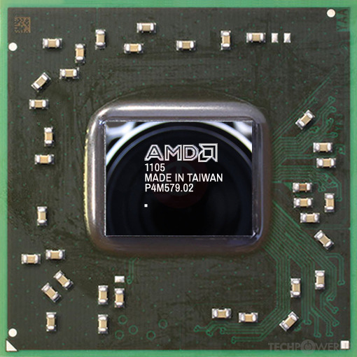
The Radeon E6465 was a mobile graphics chip by AMD, launched on September 29th, 2015. Built on the 40 nm process, and based on the Caicos graphics processor, the chip supports DirectX 11.2. The Caicos graphics processor is a relatively small chip with a die area of only 67 mm² and 370 million transistors. It features 160 shading units, 8 texture mapping units, and 4 ROPs. AMD has paired 2,048 MB GDDR5 memory with the Radeon E6465, which are connected using a 64-bit memory interface. The GPU is operating at a frequency of 600 MHz, memory is running at 800 MHz (3.2 Gbps effective).
Being a single-slot card, the AMD Radeon E6465 does not require any additional power connector, its power draw is rated at 25 W maximum. This device has no display connectivity, as it is not designed to have monitors connected to it. Rather it is intended for use in laptop/notebooks and will use the output of the host mobile device. Radeon E6465 is connected to the rest of the system using a PCI-Express 2.0 x16 interface.
Being a single-slot card, the AMD Radeon E6465 does not require any additional power connector, its power draw is rated at 25 W maximum. This device has no display connectivity, as it is not designed to have monitors connected to it. Rather it is intended for use in laptop/notebooks and will use the output of the host mobile device. Radeon E6465 is connected to the rest of the system using a PCI-Express 2.0 x16 interface.
Graphics Processor
- GPU Name
- Caicos
- Architecture
- TeraScale 2
- Foundry
- TSMC
- Process Size
- 40 nm
- Transistors
- 370 million
- Density
- 5.5M / mm²
- Die Size
- 67 mm²
- Chip Package
- FCBGA-631
Mobile Graphics
- Release Date
- Sep 29th, 2015
- Generation
-
Embedded
(6000)
- Production
- End-of-life
- Bus Interface
- PCIe 2.0 x16
Relative Performance
Based on TPU review data: "Performance Summary" at 1920x1080, 4K for 2080 Ti and faster.
Performance estimated based on architecture, shader count and clocks.
Clock Speeds
- GPU Clock
- 600 MHz
- Memory Clock
-
800 MHz
3.2 Gbps effective
Memory
- Memory Size
- 2 GB
- Memory Type
- GDDR5
- Memory Bus
- 64 bit
- Bandwidth
- 25.60 GB/s
Render Config
- Shading Units
- 160
- TMUs
- 8
- ROPs
- 4
- Compute Units
- 2
- L1 Cache
- 8 KB (per CU)
- L2 Cache
- 128 KB
Theoretical Performance
- Pixel Rate
- 2.400 GPixel/s
- Texture Rate
- 4.800 GTexel/s
- FP32 (float)
- 192.0 GFLOPS
Board Design
- Slot Width
- Single-slot
- TDP
- 25 W
- Outputs
- Portable Device Dependent
- Power Connectors
- None
- Board Number
- 109-C91147-00_04
Graphics Features
- DirectX
- 11.2 (11_0)
- OpenGL
- 4.4
- OpenCL
- 1.2
- Vulkan
- N/A
- Shader Model
- 5.0
Card Notes
| Used In Embedded PCs |
Caicos GPU Notes
| Generation: Northern Islands Mobile Variant: Seymour Graphics/Compute: GFX4 Display Core Engine: 5.0 Unified Video Decoder: 3.1 |
Devices based on this design (1)
| Name | GPU Clock | Memory Clock | Other Changes |
|---|---|---|---|
| 600 MHz | 800 MHz | 4x mini-DisplayPort |

Apr 25th, 2024 00:26 EDT
change timezone
Latest GPU Drivers
New Forum Posts
- What's your latest tech purchase? (20337)
- The Official Linux/Unix Desktop Screenshots Megathread (694)
- XFX RX470 8GB no video and error 43 (27)
- (Anti) SFF fun house (348)
- Cinebench crashed my PC. My Wi-Fi stopped working, and I keep getting a "Please wait" screen when I boot up my PC. (31)
- im new to throttelstop and i think i messed it up by copying others any hints would be very much aprreciated (1)
- Aida64 cache mem OC (7)
- I am getting artifacting when I change Windows security settings. Is my GPU failing, or is this just a Windows issue? (10)
- Is there a technical reason that Windows 11 doesn't have built into it battery charge limitation? (42)
- The TPU UK Clubhouse (24783)
Popular Reviews
- Fractal Design Terra Review
- Thermalright Phantom Spirit 120 EVO Review
- Corsair 2000D Airflow Review
- Minisforum EliteMini UM780 XTX (AMD Ryzen 7 7840HS) Review
- ASUS GeForce RTX 4090 STRIX OC Review
- NVIDIA GeForce RTX 4090 Founders Edition Review - Impressive Performance
- ASUS GeForce RTX 4090 Matrix Platinum Review - The RTX 4090 Ti
- MSI GeForce RTX 4090 Suprim X Review
- MSI GeForce RTX 4090 Gaming X Trio Review
- Gigabyte GeForce RTX 4090 Gaming OC Review
Controversial News Posts
- Sony PlayStation 5 Pro Specifications Confirmed, Console Arrives Before Holidays (116)
- NVIDIA Points Intel Raptor Lake CPU Users to Get Help from Intel Amid System Instability Issues (106)
- AMD "Strix Halo" Zen 5 Mobile Processor Pictured: Chiplet-based, Uses 256-bit LPDDR5X (101)
- US Government Wants Nuclear Plants to Offload AI Data Center Expansion (98)
- Windows 10 Security Updates to Cost $61 After 2025, $427 by 2028 (84)
- Developers of Outpost Infinity Siege Recommend Underclocking i9-13900K and i9-14900K for Stability on Machines with RTX 4090 (84)
- TechPowerUp Hiring: Reviewers Wanted for Motherboards, Laptops, Gaming Handhelds and Prebuilt Desktops (78)
- AMD's RDNA 4 GPUs Could Stick with 18 Gbps GDDR6 Memory (73)