Report an Error


NVIDIA GeForce GTX 590
- Graphics Processor
- GF110 x2
- Cores
- 512 x2
- TMUs
- 64 x2
- ROPs
- 48 x2
- Memory Size
- 1536 MB x2
- Memory Type
- GDDR5
- Bus Width
- 384 bit x2

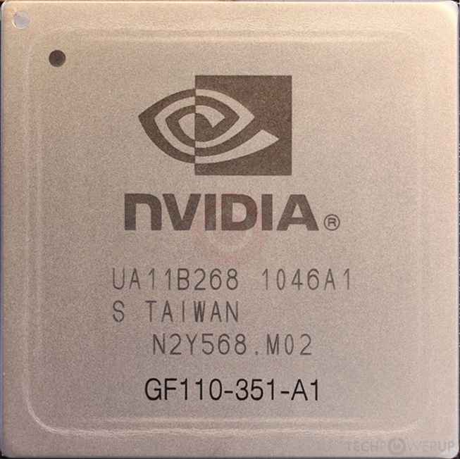
GPU

I/O
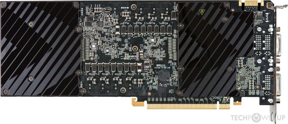
Back

PCB Front
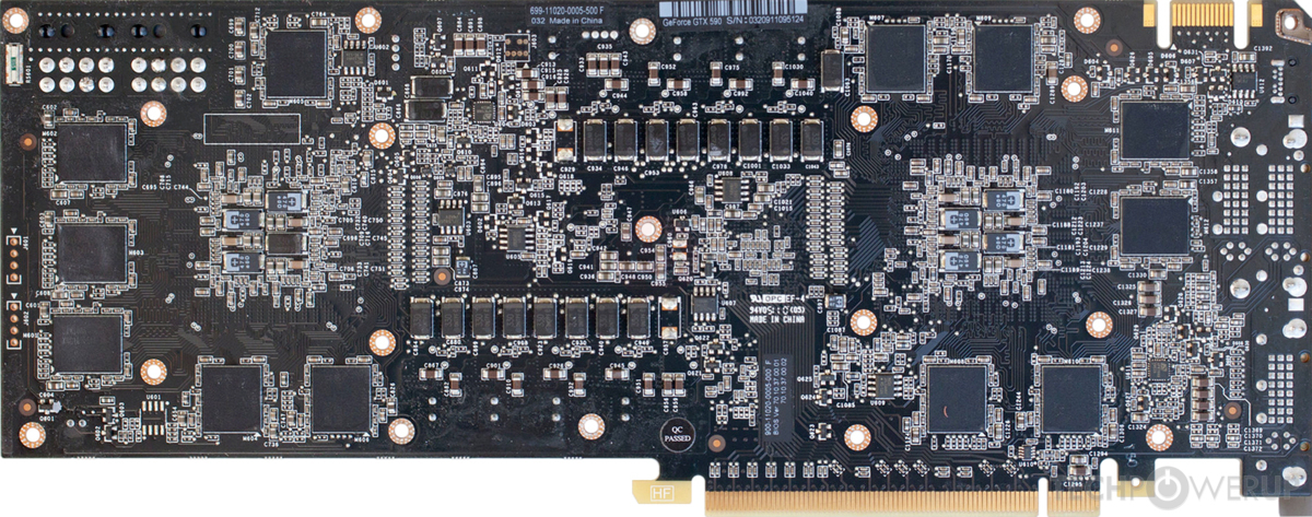
PCB Back
Recommended Gaming Resolutions:
- 1600x900
- 1920x1080
- 2560x1440
The GeForce GTX 590 was an enthusiast-class graphics card by NVIDIA, launched on March 24th, 2011. Built on the 40 nm process, and based on the GF110 graphics processor, in its GF110-351-A1 variant, the card supports DirectX 12. Even though it supports DirectX 12, the feature level is only 11_0, which can be problematic with newer DirectX 12 titles. The GF110 graphics processor is a large chip with a die area of 520 mm² and 3,000 million transistors. GeForce GTX 590 combines two graphics processors to increase performance. It features 512 shading units, 64 texture mapping units, and 48 ROPs, per GPU. NVIDIA has paired 3,072 MB GDDR5 memory with the GeForce GTX 590, which are connected using a 384-bit memory interface per GPU (each GPU manages 1,536 MB). The GPU is operating at a frequency of 608 MHz, memory is running at 854 MHz (3.4 Gbps effective).
Being a dual-slot card, the NVIDIA GeForce GTX 590 draws power from 2x 8-pin power connectors, with power draw rated at 365 W maximum. Display outputs include: 3x DVI, 1x mini-DisplayPort. GeForce GTX 590 is connected to the rest of the system using a PCI-Express 2.0 x16 interface. The card's dimensions are 279 mm x 111 mm x 40 mm, and it features a dual-slot cooling solution. Its price at launch was 699 US Dollars.
Being a dual-slot card, the NVIDIA GeForce GTX 590 draws power from 2x 8-pin power connectors, with power draw rated at 365 W maximum. Display outputs include: 3x DVI, 1x mini-DisplayPort. GeForce GTX 590 is connected to the rest of the system using a PCI-Express 2.0 x16 interface. The card's dimensions are 279 mm x 111 mm x 40 mm, and it features a dual-slot cooling solution. Its price at launch was 699 US Dollars.
Graphics Processor
Graphics Card
- Release Date
- Mar 24th, 2011
- Generation
- GeForce 500
- Predecessor
- GeForce 400
- Successor
- GeForce 600
- Production
- End-of-life
- Launch Price
- 699 USD
- Bus Interface
- PCIe 2.0 x16
- Reviews
- 36 in our database
Relative Performance
Based on TPU review data: "Performance Summary" at 1920x1080, 4K for 2080 Ti and faster.
Clock Speeds
- GPU Clock
- 608 MHz
- Shader Clock
- 1215 MHz
- Memory Clock
-
854 MHz
3.4 Gbps effective
Memory
- Memory Size
- 1536 MB
- Memory Type
- GDDR5
- Memory Bus
- 384 bit
- Bandwidth
- 164.0 GB/s
Render Config
- Shading Units
- 512
- TMUs
- 64
- ROPs
- 48
- SM Count
- 16
- L1 Cache
- 64 KB (per SM)
- L2 Cache
- 768 KB
Theoretical Performance
- Pixel Rate
- 19.46 GPixel/s
- Texture Rate
- 38.91 GTexel/s
- FP32 (float)
- 1,244 GFLOPS
- FP64 (double)
- 155.5 GFLOPS (1:8)
Board Design
- Slot Width
- Dual-slot
- Length
- 279 mm
11 inches
- Width
- 111 mm
4.4 inches
- Height
- 40 mm
1.6 inches
- TDP
- 365 W
- Suggested PSU
- 750 W
- Outputs
- 3x DVI
1x mini-DisplayPort
- Power Connectors
- 2x 8-pin
- Board Number
- P1020 SKU 5
Graphics Features
- DirectX
- 12 (11_0)
- OpenGL
- 4.6
- OpenCL
- 1.1
- Vulkan
- N/A
- CUDA
- 2.0
- Shader Model
- 5.1
Card Notes
| Dual GPU design, 2x GF110 |
GF110 GPU Notes
| PureVideo HD: VP4 VDPAU: Feature Set C GF110 has 4 GPCs each capable of 8 pixels per clock. This limits complete GPU to 32 pixels per clock and because of that it can't feed all 48 ROPs when they all require data at the same time. Additional ROPs however can be used for MSAA (because it doesn't require additional data from rasterizers, while giving more work to ROPs.) The complete die contains 64 texture address units and 256 texture filtering units. |
Retail boards based on this design (9)
| Name | GPU Clock | Memory Clock | Other Changes |
|---|---|---|---|
| 782 MHz | 1002 MHz | 330 mm/13 inches, Triple-slot, 2x DVI 1x HDMI 1x DisplayPort | |
| 608 MHz | 854 MHz | ||
| 630 MHz | 864 MHz | ||
| 630 MHz | 864 MHz | ||
| 608 MHz | 854 MHz | ||
| 641 MHz | 907 MHz | ||
| 692 MHz | 928 MHz | ||
| 671 MHz | 854 MHz | ||
| 608 MHz | 854 MHz |


Apr 25th, 2024 07:31 EDT
change timezone
Latest GPU Drivers
New Forum Posts
- (Anti) SFF fun house (353)
- Core i5-6300U (17)
- Last game you purchased? (255)
- Share your AIDA 64 cache and memory benchmark here (2916)
- What phone you use as your daily driver? And, a discussion of them. (1472)
- What's your latest tech purchase? (20338)
- Meta Horizon OS (16)
- Alphacool CORE 1 CPU block - bulging with danger of splitting? (4)
- The TPU UK Clubhouse (24786)
- Github comments used to push malware via Microsoft repo urls (3)
Popular Reviews
- Fractal Design Terra Review
- Thermalright Phantom Spirit 120 EVO Review
- Corsair 2000D Airflow Review
- Minisforum EliteMini UM780 XTX (AMD Ryzen 7 7840HS) Review
- ASUS GeForce RTX 4090 STRIX OC Review
- NVIDIA GeForce RTX 4090 Founders Edition Review - Impressive Performance
- ASUS GeForce RTX 4090 Matrix Platinum Review - The RTX 4090 Ti
- MSI GeForce RTX 4090 Suprim X Review
- MSI GeForce RTX 4090 Gaming X Trio Review
- Gigabyte GeForce RTX 4090 Gaming OC Review
Controversial News Posts
- Sony PlayStation 5 Pro Specifications Confirmed, Console Arrives Before Holidays (116)
- NVIDIA Points Intel Raptor Lake CPU Users to Get Help from Intel Amid System Instability Issues (106)
- AMD "Strix Halo" Zen 5 Mobile Processor Pictured: Chiplet-based, Uses 256-bit LPDDR5X (101)
- US Government Wants Nuclear Plants to Offload AI Data Center Expansion (98)
- Windows 11 Now Officially Adware as Microsoft Embeds Ads in the Start Menu (86)
- Windows 10 Security Updates to Cost $61 After 2025, $427 by 2028 (84)
- Developers of Outpost Infinity Siege Recommend Underclocking i9-13900K and i9-14900K for Stability on Machines with RTX 4090 (84)
- AMD's RDNA 4 GPUs Could Stick with 18 Gbps GDDR6 Memory (80)