Report an Error


NVIDIA GeForce GTX 470 X2
- Graphics Processor
- GF100 x2
- Cores
- 352 x2
- TMUs
- 44 x2
- ROPs
- 32 x2
- Memory Size
- 1024 MB x2
- Memory Type
- GDDR5
- Bus Width
- 256 bit x2

GPU
Recommended Gaming Resolutions:
- 1600x900
- 1920x1080
- 2560x1440
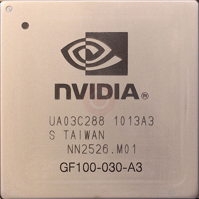
The GeForce GTX 470 X2 was a graphics card by NVIDIA, that was never released. Built on the 40 nm process, and based on the GF100 graphics processor, in its GF100-030-A3 variant, the card supports DirectX 12. Even though it supports DirectX 12, the feature level is only 11_0, which can be problematic with newer DirectX 12 titles. The GF100 graphics processor is a large chip with a die area of 529 mm² and 3,100 million transistors. Unlike the fully unlocked GeForce GTX 480 Core 512, which uses the same GPU but has all 512 shaders enabled, NVIDIA has disabled some shading units on the GeForce GTX 470 X2 to reach the product's target shader count. GeForce GTX 470 X2 combines two graphics processors to increase performance. It features 352 shading units, 44 texture mapping units, and 32 ROPs, per GPU. NVIDIA has paired 2,048 MB GDDR5 memory with the GeForce GTX 470 X2, which are connected using a 256-bit memory interface per GPU (each GPU manages 1,024 MB). The GPU is operating at a frequency of 608 MHz, memory is running at 837 MHz (3.3 Gbps effective).
Being a dual-slot card, the NVIDIA GeForce GTX 470 X2 draws power from 2x 8-pin power connectors, with power draw rated at 215 W maximum. Display outputs include: 3x DVI. GeForce GTX 470 X2 is connected to the rest of the system using a PCI-Express 2.0 x16 interface.
Being a dual-slot card, the NVIDIA GeForce GTX 470 X2 draws power from 2x 8-pin power connectors, with power draw rated at 215 W maximum. Display outputs include: 3x DVI. GeForce GTX 470 X2 is connected to the rest of the system using a PCI-Express 2.0 x16 interface.
Graphics Processor
Graphics Card
- Release Date
- Never Released
- Generation
- GeForce 400
- Predecessor
- GeForce 200
- Successor
- GeForce 500
- Production
- End-of-life
- Bus Interface
- PCIe 2.0 x16
- Reviews
- 48 in our database
Relative Performance
Based on TPU review data: "Performance Summary" at 1920x1080, 4K for 2080 Ti and faster.
Performance estimated based on architecture, shader count and clocks.
Clock Speeds
- GPU Clock
- 608 MHz
- Shader Clock
- 1215 MHz
- Memory Clock
-
837 MHz
3.3 Gbps effective
Memory
- Memory Size
- 1024 MB
- Memory Type
- GDDR5
- Memory Bus
- 256 bit
- Bandwidth
- 107.1 GB/s
Render Config
- Shading Units
- 352
- TMUs
- 44
- ROPs
- 32
- SM Count
- 11
- L1 Cache
- 64 KB (per SM)
- L2 Cache
- 512 KB
Theoretical Performance
- Pixel Rate
- 13.38 GPixel/s
- Texture Rate
- 26.75 GTexel/s
- FP32 (float)
- 855.4 GFLOPS
Board Design
- Slot Width
- Dual-slot
- TDP
- 215 W
- Suggested PSU
- 550 W
- Outputs
- 3x DVI
- Power Connectors
- 2x 8-pin
Graphics Features
- DirectX
- 12 (11_0)
- OpenGL
- 4.6
- OpenCL
- 1.1
- Vulkan
- N/A
- CUDA
- 2.0
- Shader Model
- 5.1
GF100 GPU Notes
| PureVideo HD: VP4 VDPAU: Feature Set C GF100 has 4 GPCs each capable of 8 pixels per clock. This limits complete GPU to 32 pixels per clock and because of that it can't feed all 48 ROPs when they all require data at the same time. Additional ROPs however can be used for MSAA (because it doesn't require additional data from rasterizers, while giving more work to ROPs.) |
Retail boards based on this design (1)
| Name | GPU Clock | Memory Clock | Other Changes |
|---|---|---|---|
| 608 MHz | 837 MHz |

Apr 25th, 2024 02:31 EDT
change timezone
Latest GPU Drivers
New Forum Posts
- What phone you use as your daily driver? And, a discussion of them. (1471)
- Core i5-6300U (12)
- Github comments used to push malware via Microsoft repo urls (2)
- The TPU UK Clubhouse (24784)
- (Anti) SFF fun house (349)
- What's your latest tech purchase? (20337)
- The Official Linux/Unix Desktop Screenshots Megathread (694)
- XFX RX470 8GB no video and error 43 (27)
- Cinebench crashed my PC. My Wi-Fi stopped working, and I keep getting a "Please wait" screen when I boot up my PC. (31)
- im new to throttelstop and i think i messed it up by copying others any hints would be very much aprreciated (1)
Popular Reviews
- Fractal Design Terra Review
- Thermalright Phantom Spirit 120 EVO Review
- Corsair 2000D Airflow Review
- Minisforum EliteMini UM780 XTX (AMD Ryzen 7 7840HS) Review
- ASUS GeForce RTX 4090 STRIX OC Review
- NVIDIA GeForce RTX 4090 Founders Edition Review - Impressive Performance
- ASUS GeForce RTX 4090 Matrix Platinum Review - The RTX 4090 Ti
- MSI GeForce RTX 4090 Suprim X Review
- MSI GeForce RTX 4090 Gaming X Trio Review
- Gigabyte GeForce RTX 4090 Gaming OC Review
Controversial News Posts
- Sony PlayStation 5 Pro Specifications Confirmed, Console Arrives Before Holidays (116)
- NVIDIA Points Intel Raptor Lake CPU Users to Get Help from Intel Amid System Instability Issues (106)
- AMD "Strix Halo" Zen 5 Mobile Processor Pictured: Chiplet-based, Uses 256-bit LPDDR5X (101)
- US Government Wants Nuclear Plants to Offload AI Data Center Expansion (98)
- Windows 10 Security Updates to Cost $61 After 2025, $427 by 2028 (84)
- Developers of Outpost Infinity Siege Recommend Underclocking i9-13900K and i9-14900K for Stability on Machines with RTX 4090 (84)
- TechPowerUp Hiring: Reviewers Wanted for Motherboards, Laptops, Gaming Handhelds and Prebuilt Desktops (78)
- AMD's RDNA 4 GPUs Could Stick with 18 Gbps GDDR6 Memory (74)