Report an Error


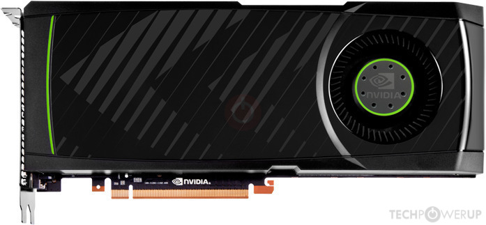
NVIDIA GeForce GTX 580 Rev. 2
- Graphics Processor
- GF110
- Cores
- 512
- TMUs
- 64
- ROPs
- 48
- Memory Size
- 1536 MB
- Memory Type
- GDDR5
- Bus Width
- 384 bit

GPU

I/O
Recommended Gaming Resolutions:
- 1600x900
- 1920x1080
- 2560x1440
The GeForce GTX 580 Rev. 2 was a high-end graphics card by NVIDIA, launched on June 6th, 2011. Built on the 40 nm process, and based on the GF110 graphics processor, in its GF110-380-A1 variant, the card supports DirectX 12. Even though it supports DirectX 12, the feature level is only 11_0, which can be problematic with newer DirectX 12 titles. The GF110 graphics processor is a large chip with a die area of 520 mm² and 3,000 million transistors. It features 512 shading units, 64 texture mapping units, and 48 ROPs. NVIDIA has paired 1,536 MB GDDR5 memory with the GeForce GTX 580 Rev. 2, which are connected using a 384-bit memory interface. The GPU is operating at a frequency of 772 MHz, memory is running at 1002 MHz (4 Gbps effective).
Being a dual-slot card, the NVIDIA GeForce GTX 580 Rev. 2 draws power from 1x 6-pin + 1x 8-pin power connector, with power draw rated at 244 W maximum. Display outputs include: 2x DVI, 1x mini-HDMI 1.3a. GeForce GTX 580 Rev. 2 is connected to the rest of the system using a PCI-Express 2.0 x16 interface. The card measures 267 mm in length, and features a dual-slot cooling solution. Its price at launch was 499 US Dollars.
Being a dual-slot card, the NVIDIA GeForce GTX 580 Rev. 2 draws power from 1x 6-pin + 1x 8-pin power connector, with power draw rated at 244 W maximum. Display outputs include: 2x DVI, 1x mini-HDMI 1.3a. GeForce GTX 580 Rev. 2 is connected to the rest of the system using a PCI-Express 2.0 x16 interface. The card measures 267 mm in length, and features a dual-slot cooling solution. Its price at launch was 499 US Dollars.
Graphics Processor
Graphics Card
- Release Date
- Jun 6th, 2011
- Generation
- GeForce 500
- Predecessor
- GeForce 400
- Successor
- GeForce 600
- Production
- End-of-life
- Launch Price
- 499 USD
- Bus Interface
- PCIe 2.0 x16
- Reviews
- 136 in our database
Relative Performance
Based on TPU review data: "Performance Summary" at 1920x1080, 4K for 2080 Ti and faster.
Performance estimated based on architecture, shader count and clocks.
Clock Speeds
- GPU Clock
- 772 MHz
- Shader Clock
- 1544 MHz
- Memory Clock
-
1002 MHz
4 Gbps effective
Memory
- Memory Size
- 1536 MB
- Memory Type
- GDDR5
- Memory Bus
- 384 bit
- Bandwidth
- 192.4 GB/s
Render Config
- Shading Units
- 512
- TMUs
- 64
- ROPs
- 48
- SM Count
- 16
- L1 Cache
- 64 KB (per SM)
- L2 Cache
- 768 KB
Theoretical Performance
- Pixel Rate
- 24.70 GPixel/s
- Texture Rate
- 49.41 GTexel/s
- FP32 (float)
- 1.581 TFLOPS
- FP64 (double)
- 197.6 GFLOPS (1:8)
Board Design
- Slot Width
- Dual-slot
- Length
- 267 mm
10.5 inches
- TDP
- 244 W
- Suggested PSU
- 550 W
- Outputs
- 2x DVI
1x mini-HDMI 1.3a
- Power Connectors
- 1x 6-pin + 1x 8-pin
- Board Number
- P1261 SKU 12
Graphics Features
- DirectX
- 12 (11_0)
- OpenGL
- 4.6
- OpenCL
- 1.1
- Vulkan
- N/A
- CUDA
- 2.0
- Shader Model
- 5.1
GF110 GPU Notes
| PureVideo HD: VP4 VDPAU: Feature Set C GF110 has 4 GPCs each capable of 8 pixels per clock. This limits complete GPU to 32 pixels per clock and because of that it can't feed all 48 ROPs when they all require data at the same time. Additional ROPs however can be used for MSAA (because it doesn't require additional data from rasterizers, while giving more work to ROPs.) The complete die contains 64 texture address units and 256 texture filtering units. |
Apr 23rd, 2024 20:34 EDT
change timezone
Latest GPU Drivers
New Forum Posts
- What's your latest tech purchase? (20319)
- Post your Cinebench 2024 score (449)
- Sexy Mechanical Keyboard Thread (484)
- The TPU UK Clubhouse (24766)
- need help with motherboard/ ram compability certainty (14)
- My computer setup - Request for opinions (12)
- Show us your collections thread!! (282)
- Realtek Modded Audio Driver for Windows 10/11 - Only for HDAUDIO (5687)
- What phone you use as your daily driver? And, a discussion of them. (1454)
- Is there a technical reason that Windows 11 doesn't have built into it battery charge limitation? (37)
Popular Reviews
- Fractal Design Terra Review
- Corsair 2000D Airflow Review
- Thermalright Phantom Spirit 120 EVO Review
- Minisforum EliteMini UM780 XTX (AMD Ryzen 7 7840HS) Review
- ASUS GeForce RTX 4090 STRIX OC Review
- NVIDIA GeForce RTX 4090 Founders Edition Review - Impressive Performance
- ASUS GeForce RTX 4090 Matrix Platinum Review - The RTX 4090 Ti
- MSI GeForce RTX 4090 Gaming X Trio Review
- MSI GeForce RTX 4090 Suprim X Review
- Gigabyte GeForce RTX 4090 Gaming OC Review
Controversial News Posts
- Sony PlayStation 5 Pro Specifications Confirmed, Console Arrives Before Holidays (116)
- NVIDIA Points Intel Raptor Lake CPU Users to Get Help from Intel Amid System Instability Issues (106)
- AMD "Strix Halo" Zen 5 Mobile Processor Pictured: Chiplet-based, Uses 256-bit LPDDR5X (101)
- US Government Wants Nuclear Plants to Offload AI Data Center Expansion (98)
- Windows 10 Security Updates to Cost $61 After 2025, $427 by 2028 (84)
- Developers of Outpost Infinity Siege Recommend Underclocking i9-13900K and i9-14900K for Stability on Machines with RTX 4090 (84)
- TechPowerUp Hiring: Reviewers Wanted for Motherboards, Laptops, Gaming Handhelds and Prebuilt Desktops (74)
- Intel Realizes the Only Way to Save x86 is to Democratize it, Reopens x86 IP Licensing (70)