Report an Error


NVIDIA GeForce GTS 450 OEM
- Graphics Processor
- GF106
- Cores
- 144
- TMUs
- 24
- ROPs
- 16
- Memory Size
- 512 MB
- Memory Type
- GDDR5
- Bus Width
- 128 bit

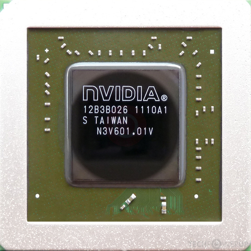
GPU
Recommended Gaming Resolutions:
- 1280x720
- 1366x768
- 1600x900
The GeForce GTS 450 OEM was a mid-range graphics card by NVIDIA, launched on September 13th, 2010. Built on the 40 nm process, and based on the GF106 graphics processor, the card supports DirectX 12. Even though it supports DirectX 12, the feature level is only 11_0, which can be problematic with newer DirectX 12 titles. The GF106 graphics processor is an average sized chip with a die area of 238 mm² and 1,170 million transistors. Unlike the fully unlocked GeForce GTS 450, which uses the same GPU but has all 192 shaders enabled, NVIDIA has disabled some shading units on the GeForce GTS 450 OEM to reach the product's target shader count. It features 144 shading units, 24 texture mapping units, and 16 ROPs. NVIDIA has paired 512 MB GDDR5 memory with the GeForce GTS 450 OEM, which are connected using a 128-bit memory interface. The GPU is operating at a frequency of 783 MHz, memory is running at 902 MHz (3.6 Gbps effective).
Being a single-slot card, the NVIDIA GeForce GTS 450 OEM draws power from 1x 6-pin power connector, with power draw rated at 106 W maximum. Display outputs include: 1x DVI, 1x DisplayPort, 1x VGA. GeForce GTS 450 OEM is connected to the rest of the system using a PCI-Express 2.0 x16 interface. The card measures 210 mm in length, and features a single-slot cooling solution. Its price at launch was 129 US Dollars.
Being a single-slot card, the NVIDIA GeForce GTS 450 OEM draws power from 1x 6-pin power connector, with power draw rated at 106 W maximum. Display outputs include: 1x DVI, 1x DisplayPort, 1x VGA. GeForce GTS 450 OEM is connected to the rest of the system using a PCI-Express 2.0 x16 interface. The card measures 210 mm in length, and features a single-slot cooling solution. Its price at launch was 129 US Dollars.
Graphics Processor
Graphics Card
- Release Date
- Sep 13th, 2010
- Generation
- GeForce 400
- Predecessor
- GeForce 200
- Successor
- GeForce 500
- Production
- End-of-life
- Launch Price
- 129 USD
- Bus Interface
- PCIe 2.0 x16
- Reviews
- 80 in our database
Relative Performance
Based on TPU review data: "Performance Summary" at 1920x1080, 4K for 2080 Ti and faster.
Performance estimated based on architecture, shader count and clocks.
Clock Speeds
- GPU Clock
- 783 MHz
- Shader Clock
- 1566 MHz
- Memory Clock
-
902 MHz
3.6 Gbps effective
Memory
- Memory Size
- 512 MB
- Memory Type
- GDDR5
- Memory Bus
- 128 bit
- Bandwidth
- 57.73 GB/s
Render Config
- Shading Units
- 144
- TMUs
- 24
- ROPs
- 16
- SM Count
- 3
- L1 Cache
- 64 KB (per SM)
- L2 Cache
- 256 KB
Theoretical Performance
- Pixel Rate
- 4.698 GPixel/s
- Texture Rate
- 18.79 GTexel/s
- FP32 (float)
- 451.0 GFLOPS
- FP64 (double)
- 37.58 GFLOPS (1:12)
Board Design
- Slot Width
- Single-slot
- Length
- 210 mm
8.3 inches
- TDP
- 106 W
- Suggested PSU
- 300 W
- Outputs
- 1x DVI
1x DisplayPort
1x VGA
- Power Connectors
- 1x 6-pin
- Board Number
- P1060 SKU 11
Graphics Features
- DirectX
- 12 (11_0)
- OpenGL
- 4.6
- OpenCL
- 1.1
- Vulkan
- N/A
- CUDA
- 2.1
- Shader Model
- 5.1
GF106 GPU Notes
| PureVideo HD: VP4 VDPAU: Feature Set C |
Retail boards based on this design (1)
| Name | GPU Clock | Memory Clock | Other Changes |
|---|---|---|---|
| 783 MHz | 902 MHz |

Apr 17th, 2024 20:22 EDT
change timezone
Latest GPU Drivers
New Forum Posts
- The TPU UK Clubhouse (24722)
- Sold my a working PSU that I have been using, but buyer says it sparked at the outlet when he plugged it in and asking for a possible refund (8)
- Gigabyte gpu model differences? (25)
- What's your latest tech purchase? (20252)
- FINAL FANTASY XIV: Dawntrail Official Benchmark (43)
- Free Games Thread (3763)
- What are you playing? (20450)
- Dell Poweredge t610 into gaming pc (62)
- Why do i have such a huge Thread(?) usage imbalance (6)
- Easy mistake - Easy fix (47)
Popular Reviews
- Horizon Forbidden West Performance Benchmark Review - 30 GPUs Tested
- PowerColor Radeon RX 7900 GRE Hellhound Review
- Fractal Design Terra Review
- ASUS GeForce RTX 4090 Matrix Platinum Review - The RTX 4090 Ti
- Corsair 2000D Airflow Review
- Minisforum EliteMini UM780 XTX (AMD Ryzen 7 7840HS) Review
- Creative Pebble X Plus Review
- FiiO KB3 HiFi Mechanical Keyboard Review - Integrated DAC/Amp!
- ASUS GeForce RTX 4090 STRIX OC Review
- NVIDIA GeForce RTX 4090 Founders Edition Review - Impressive Performance
Controversial News Posts
- Sony PlayStation 5 Pro Specifications Confirmed, Console Arrives Before Holidays (104)
- NVIDIA Points Intel Raptor Lake CPU Users to Get Help from Intel Amid System Instability Issues (102)
- US Government Wants Nuclear Plants to Offload AI Data Center Expansion (98)
- Windows 10 Security Updates to Cost $61 After 2025, $427 by 2028 (82)
- Developers of Outpost Infinity Siege Recommend Underclocking i9-13900K and i9-14900K for Stability on Machines with RTX 4090 (82)
- TechPowerUp Hiring: Reviewers Wanted for Motherboards, Laptops, Gaming Handhelds and Prebuilt Desktops (70)
- Intel Realizes the Only Way to Save x86 is to Democratize it, Reopens x86 IP Licensing (70)
- AMD Zen 5 Execution Engine Leaked, Features True 512-bit FPU (63)