Report an Error


AMD Radeon HD 6730M
- Graphics Processor
- Whistler
- Cores
- 480
- TMUs
- 24
- ROPs
- 8
- Memory Size
- 1024 MB
- Memory Type
- GDDR3
- Bus Width
- 128 bit
GPU
Recommended Gaming Resolutions:
- 1366x768
- 1600x900
- 1920x1080
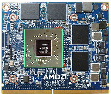
The Radeon HD 6730M was a mobile graphics chip by AMD, launched on January 4th, 2011. Built on the 40 nm process, and based on the Whistler graphics processor, in its Whistler LE variant, the chip supports DirectX 11.2. The Whistler graphics processor is an average sized chip with a die area of 118 mm² and 716 million transistors. It features 480 shading units, 24 texture mapping units, and 8 ROPs. AMD has paired 1,024 MB GDDR3 memory with the Radeon HD 6730M, which are connected using a 128-bit memory interface. The GPU is operating at a frequency of 725 MHz, memory is running at 800 MHz.
Being a mxm module card, its power draw is rated at 35 W maximum. This device has no display connectivity, as it is not designed to have monitors connected to it. Rather it is intended for use in laptop/notebooks and will use the output of the host mobile device.
Being a mxm module card, its power draw is rated at 35 W maximum. This device has no display connectivity, as it is not designed to have monitors connected to it. Rather it is intended for use in laptop/notebooks and will use the output of the host mobile device.
Graphics Processor
- GPU Name
- Whistler
- GPU Variant
-
Whistler LE
(216-0810028)
- Architecture
- TeraScale 2
- Foundry
- TSMC
- Process Size
- 40 nm
- Transistors
- 716 million
- Density
- 6.1M / mm²
- Die Size
- 118 mm²
- Chip Package
- FCBGA-962/1336
Mobile Graphics
Relative Performance
Based on TPU review data: "Performance Summary" at 1920x1080, 4K for 2080 Ti and faster.
Performance estimated based on architecture, shader count and clocks.
Clock Speeds
- GPU Clock
- 725 MHz
- Memory Clock
-
800 MHz
1600 Mbps effective
Memory
- Memory Size
- 1024 MB
- Memory Type
- GDDR3
- Memory Bus
- 128 bit
- Bandwidth
- 25.60 GB/s
Render Config
- Shading Units
- 480
- TMUs
- 24
- ROPs
- 8
- Compute Units
- 6
- L1 Cache
- 8 KB (per CU)
- L2 Cache
- 256 KB
Theoretical Performance
- Pixel Rate
- 5.800 GPixel/s
- Texture Rate
- 17.40 GTexel/s
- FP32 (float)
- 696.0 GFLOPS
Board Design
- Slot Width
- MXM Module
- TDP
- 35 W
- Outputs
- Portable Device Dependent
Graphics Features
- DirectX
- 11.2 (11_0)
- OpenGL
- 4.4
- OpenCL
- 1.2
- Vulkan
- N/A
- Shader Model
- 5.0
Whistler GPU Notes
| Generation: Northern Islands Desktop Variant: Turks Mobile Variant: Thames Graphics/Compute: GFX4 Display Core Engine: 5.0 Unified Video Decoder: 3.1 |
Devices based on this design (1)
| Name | GPU Clock | Memory Clock | Other Changes |
|---|---|---|---|
| 725 MHz | 800 MHz | 2 GB |

Apr 25th, 2024 06:26 EDT
change timezone
Latest GPU Drivers
New Forum Posts
- Share your AIDA 64 cache and memory benchmark here (2916)
- Last game you purchased? (254)
- What phone you use as your daily driver? And, a discussion of them. (1472)
- What's your latest tech purchase? (20338)
- Meta Horizon OS (16)
- Core i5-6300U (14)
- (Anti) SFF fun house (351)
- Alphacool CORE 1 CPU block - bulging with danger of splitting? (4)
- The TPU UK Clubhouse (24786)
- Github comments used to push malware via Microsoft repo urls (3)
Popular Reviews
- Fractal Design Terra Review
- Thermalright Phantom Spirit 120 EVO Review
- Corsair 2000D Airflow Review
- Minisforum EliteMini UM780 XTX (AMD Ryzen 7 7840HS) Review
- ASUS GeForce RTX 4090 STRIX OC Review
- NVIDIA GeForce RTX 4090 Founders Edition Review - Impressive Performance
- ASUS GeForce RTX 4090 Matrix Platinum Review - The RTX 4090 Ti
- MSI GeForce RTX 4090 Suprim X Review
- MSI GeForce RTX 4090 Gaming X Trio Review
- Gigabyte GeForce RTX 4090 Gaming OC Review
Controversial News Posts
- Sony PlayStation 5 Pro Specifications Confirmed, Console Arrives Before Holidays (116)
- NVIDIA Points Intel Raptor Lake CPU Users to Get Help from Intel Amid System Instability Issues (106)
- AMD "Strix Halo" Zen 5 Mobile Processor Pictured: Chiplet-based, Uses 256-bit LPDDR5X (101)
- US Government Wants Nuclear Plants to Offload AI Data Center Expansion (98)
- Windows 11 Now Officially Adware as Microsoft Embeds Ads in the Start Menu (84)
- Windows 10 Security Updates to Cost $61 After 2025, $427 by 2028 (84)
- Developers of Outpost Infinity Siege Recommend Underclocking i9-13900K and i9-14900K for Stability on Machines with RTX 4090 (84)
- AMD's RDNA 4 GPUs Could Stick with 18 Gbps GDDR6 Memory (80)