Report an Error


AMD Radeon HD 6950
- Graphics Processor
- Cayman
- Cores
- 1408
- TMUs
- 88
- ROPs
- 32
- Memory Size
- 2 GB
- Memory Type
- GDDR5
- Bus Width
- 256 bit
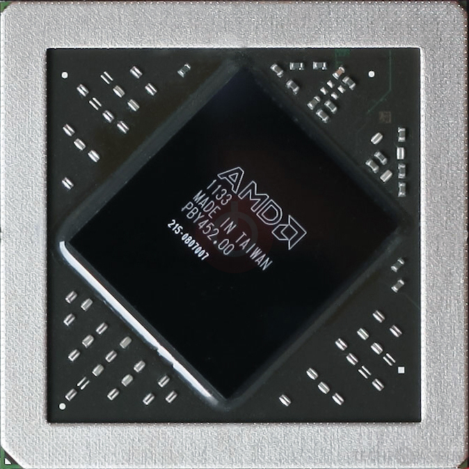
GPU

I/O

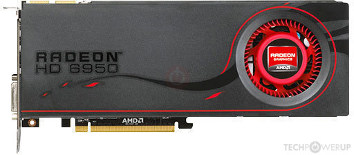
Top

PCB Front
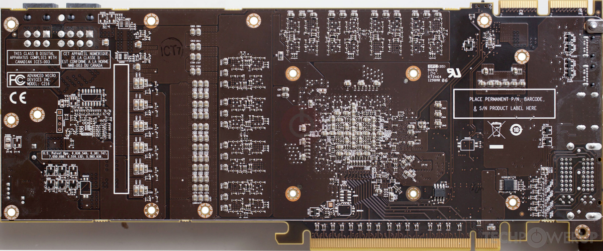
PCB Back
Recommended Gaming Resolutions:
- 1600x900
- 1920x1080
- 2560x1440
The Radeon HD 6950 was a performance-segment graphics card by AMD, launched on December 14th, 2010. Built on the 40 nm process, and based on the Cayman graphics processor, in its Cayman PRO variant, the card supports DirectX 11.2. The Cayman graphics processor is a large chip with a die area of 389 mm² and 2,640 million transistors. Unlike the fully unlocked Radeon HD 6970, which uses the same GPU but has all 1536 shaders enabled, AMD has disabled some shading units on the Radeon HD 6950 to reach the product's target shader count. It features 1408 shading units, 88 texture mapping units, and 32 ROPs. AMD has paired 2,048 MB GDDR5 memory with the Radeon HD 6950, which are connected using a 256-bit memory interface. The GPU is operating at a frequency of 800 MHz, memory is running at 1250 MHz (5 Gbps effective).
Being a dual-slot card, the AMD Radeon HD 6950 draws power from 2x 6-pin power connectors, with power draw rated at 200 W maximum. Display outputs include: 2x DVI, 1x HDMI 1.4a, 2x mini-DisplayPort 1.2. Radeon HD 6950 is connected to the rest of the system using a PCI-Express 2.0 x16 interface. The card's dimensions are 286 mm x 126 mm x 42 mm, and it features a dual-slot cooling solution. Its price at launch was 299 US Dollars.
Being a dual-slot card, the AMD Radeon HD 6950 draws power from 2x 6-pin power connectors, with power draw rated at 200 W maximum. Display outputs include: 2x DVI, 1x HDMI 1.4a, 2x mini-DisplayPort 1.2. Radeon HD 6950 is connected to the rest of the system using a PCI-Express 2.0 x16 interface. The card's dimensions are 286 mm x 126 mm x 42 mm, and it features a dual-slot cooling solution. Its price at launch was 299 US Dollars.
Graphics Processor
- GPU Name
- Cayman
- GPU Variant
-
Cayman PRO
(215-0807019)
- Architecture
- TeraScale 3
- Foundry
- TSMC
- Process Size
- 40 nm
- Transistors
- 2,640 million
- Density
- 6.8M / mm²
- Die Size
- 389 mm²
Graphics Card
- Release Date
- Dec 14th, 2010
- Generation
-
Northern Islands
(HD 6900)
- Predecessor
- Evergreen
- Successor
- Southern Islands
- Production
- End-of-life
- Launch Price
- 299 USD
- Bus Interface
- PCIe 2.0 x16
- Reviews
- 111 in our database
Relative Performance
Based on TPU review data: "Performance Summary" at 1920x1080, 4K for 2080 Ti and faster.
Clock Speeds
- GPU Clock
- 800 MHz
- Memory Clock
-
1250 MHz
5 Gbps effective
Memory
- Memory Size
- 2 GB
- Memory Type
- GDDR5
- Memory Bus
- 256 bit
- Bandwidth
- 160.0 GB/s
Render Config
- Shading Units
- 1408
- TMUs
- 88
- ROPs
- 32
- Compute Units
- 22
- L1 Cache
- 8 KB (per CU)
- L2 Cache
- 512 KB
Theoretical Performance
- Pixel Rate
- 25.60 GPixel/s
- Texture Rate
- 70.40 GTexel/s
- FP32 (float)
- 2.253 TFLOPS
- FP64 (double)
- 563.2 GFLOPS (1:4)
Board Design
- Slot Width
- Dual-slot
- Length
- 286 mm
11.3 inches
- Width
- 126 mm
5 inches
- Height
- 42 mm
1.7 inches
- TDP
- 200 W
- Suggested PSU
- 550 W
- Outputs
- 2x DVI
1x HDMI 1.4a
2x mini-DisplayPort 1.2
- Power Connectors
- 2x 6-pin
- Board Number
- 109-C21647-00
Graphics Features
- DirectX
- 11.2 (11_0)
- OpenGL
- 4.4
- OpenCL
- 1.2
- Vulkan
- N/A
- Shader Model
- 5.0
Cayman GPU Notes
| Generation: Northern Islands Desktop Variant: Antilles Graphics/Compute: GFX5 Display Core Engine: 5.0 Unified Video Decoder: 3.1 |
Retail boards based on this design (27)
| Name | GPU Clock | Memory Clock | Other Changes |
|---|---|---|---|
| 810 MHz | 1250 MHz | 297 mm/11.7 inches, Triple-slot, 2x DVI 4x DisplayPort | |
| 900 MHz | 1250 MHz | 275 mm/10.8 inches | |
| 870 MHz | 1250 MHz | 1024 MB, 290 mm/11.4 inches, 2x DVI 1x HDMI 1x DisplayPort | |
| 800 MHz | 1250 MHz | ||
| 800 MHz | 1250 MHz | 1024 MB, 255 mm/10 inches | |
| 800 MHz | 1250 MHz | 255 mm/10 inches | |
| 840 MHz | 1280 MHz | ||
| 800 MHz | 1250 MHz | 287 mm/11.3 inches | |
| 800 MHz | 1250 MHz | 1024 MB, 260 mm/10.2 inches | |
| 800 MHz | 1250 MHz | 260 mm/10.2 inches | |
| 840 MHz | 1280 MHz | 1024 MB, 260 mm/10.2 inches | |
| 840 MHz | 1280 MHz | 260 mm/10.2 inches | |
| 880 MHz | 1300 MHz | 1024 MB, 260 mm/10.2 inches | |
| 880 MHz | 1300 MHz | 260 mm/10.2 inches | |
| 810 MHz | 1250 MHz | 275 mm/10.8 inches | |
| 850 MHz | 1300 MHz | 1024 MB, 270 mm/10.6 inches | |
| 850 MHz | 1300 MHz | 270 mm/10.6 inches | |
| 880 MHz | 1250 MHz | 275 mm/10.8 inches | |
| 800 MHz | 1250 MHz | ||
| 800 MHz | 1250 MHz | 260 mm/10.2 inches, 2x DVI 1x HDMI 1x DisplayPort | |
| 800 MHz | 1250 MHz | 270 mm/10.6 inches | |
| 880 MHz | 1300 MHz | 270 mm/10.6 inches | |
| 830 MHz | 1300 MHz | 1024 MB, 256 mm/10.1 inches | |
| 830 MHz | 1300 MHz | 256 mm/10.1 inches | |
| 830 MHz | 1300 MHz | 1024 MB, 259 mm/10.2 inches | |
| 830 MHz | 1300 MHz | 259 mm/10.2 inches | |
| 800 MHz | 1250 MHz |


Apr 23rd, 2024 08:07 EDT
change timezone
Latest GPU Drivers
New Forum Posts
- Share your AIDA 64 cache and memory benchmark here (2913)
- My computer setup - Request for opinions (4)
- The best *budget* ATX PC case on the market? (23)
- Possible near-future 2024 Arrow Lake build.... (40)
- What's an inexpensive AIO product line with a strong pump and low price? (76)
- Alphacool CORE 1 CPU block - bulging with danger of splitting? (3)
- Is there a technical reason that Windows 11 doesn't have built into it battery charge limitation? (28)
- What are you playing? (20520)
- Red Dead Redemption using emu (3)
- What can be changed in a VBIOS file? (PCI vendor etc) (8)
Popular Reviews
- Horizon Forbidden West Performance Benchmark Review - 30 GPUs Tested
- Fractal Design Terra Review
- Corsair 2000D Airflow Review
- Thermalright Phantom Spirit 120 EVO Review
- Minisforum EliteMini UM780 XTX (AMD Ryzen 7 7840HS) Review
- ASUS GeForce RTX 4090 STRIX OC Review
- NVIDIA GeForce RTX 4090 Founders Edition Review - Impressive Performance
- ASUS GeForce RTX 4090 Matrix Platinum Review - The RTX 4090 Ti
- Creative Pebble X Plus Review
- MSI GeForce RTX 4090 Gaming X Trio Review
Controversial News Posts
- Sony PlayStation 5 Pro Specifications Confirmed, Console Arrives Before Holidays (116)
- NVIDIA Points Intel Raptor Lake CPU Users to Get Help from Intel Amid System Instability Issues (105)
- AMD "Strix Halo" Zen 5 Mobile Processor Pictured: Chiplet-based, Uses 256-bit LPDDR5X (101)
- US Government Wants Nuclear Plants to Offload AI Data Center Expansion (98)
- Windows 10 Security Updates to Cost $61 After 2025, $427 by 2028 (84)
- Developers of Outpost Infinity Siege Recommend Underclocking i9-13900K and i9-14900K for Stability on Machines with RTX 4090 (82)
- TechPowerUp Hiring: Reviewers Wanted for Motherboards, Laptops, Gaming Handhelds and Prebuilt Desktops (74)
- Intel Realizes the Only Way to Save x86 is to Democratize it, Reopens x86 IP Licensing (70)