Report an Error


Sapphire GT 330
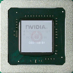
- Graphics Processor
- G92B
- Cores
- 96
- TMUs
- 48
- ROPs
- 16
- Memory Size
- 2 GB
- Memory Type
- DDR2
- Bus Width
- 128 bit

GPU
Graphics Processor
Graphics Card
- Release Date
- Feb 2nd, 2010
- Generation
- GeForce 300
- Predecessor
- GeForce 200
- Successor
- GeForce 400
- Production
- End-of-life
- Bus Interface
- PCIe 2.0 x16
Clock Speeds
- GPU Clock
- 500 MHz
- Shader Clock
- 1250 MHz
- Memory Clock
-
510 MHz
1020 Mbps effective
Memory
- Memory Size
-
256 MB
2 GB
- Memory Type
- DDR2
- Memory Bus
- 128 bit
- Bandwidth
- 16.32 GB/s
Render Config
- Shading Units
- 96
- TMUs
- 48
- ROPs
- 16
- SM Count
- 12
- L2 Cache
- 32 KB
Theoretical Performance
- Pixel Rate
- 8.000 GPixel/s
- Texture Rate
- 24.00 GTexel/s
- FP32 (float)
- 240.0 GFLOPS
Board Design
- Slot Width
- Single-slot
- TDP
- 75 W
- Suggested PSU
- 250 W
- Outputs
- 1x DVI
1x HDMI
1x VGA
- Power Connectors
- None
- Board Number
- P360 SKU 50,
P363 SKU 50
Graphics Features
- DirectX
- 11.1 (10_0)
- OpenGL
- 3.3
- OpenCL
- 1.1
- Vulkan
- N/A
- CUDA
- 1.1
- Shader Model
- 4.0
Card Notes
| Memory Variant: 512 MB Memory Variant: 768 MB Memory Variant: 2048 MB |
G92B GPU Notes
| PureVideo HD: VP2 VDPAU: Feature Set A |
Other retail boards based on this design (2)
| Name | GPU Clock | Memory Clock | Other Changes |
|---|---|---|---|
| 500 MHz | 800 MHz | 768 MB, GDDR3 | |
|
Sapphire GT 330

|
500 MHz | 510 MHz | 2 GB |

Apr 19th, 2024 14:18 EDT
change timezone
Latest GPU Drivers
New Forum Posts
- Linus watercools (40)
- TPU's WCG/BOINC Team (34420)
- I7-8750H + GTX 1050ti Laptop drops performance periodically (2)
- DDR5 RAM Speeds and the future (49)
- XFX RX470 8GB no video and error 43 (3)
- What can be changed in a VBIOS file? (PCI vendor etc) (3)
- [WIN11] 5700x3d Security processor Attestation: Not supported? (0)
- Will a RTX 4070 TI super bottleneck a Ryzen 9 7950X3D? (37)
- Do you use Linux? (254)
- Unlocked Realtek HD Audio Drivers for Windows 11 (Dolby Digital Live/DTS Interactive) (156)
Popular Reviews
- Horizon Forbidden West Performance Benchmark Review - 30 GPUs Tested
- PowerColor Radeon RX 7900 GRE Hellhound Review
- Fractal Design Terra Review
- Corsair 2000D Airflow Review
- Thermalright Phantom Spirit 120 EVO Review
- Minisforum EliteMini UM780 XTX (AMD Ryzen 7 7840HS) Review
- Creative Pebble X Plus Review
- FiiO KB3 HiFi Mechanical Keyboard Review - Integrated DAC/Amp!
- ASUS GeForce RTX 4090 STRIX OC Review
- NVIDIA GeForce RTX 4090 Founders Edition Review - Impressive Performance
Controversial News Posts
- Sony PlayStation 5 Pro Specifications Confirmed, Console Arrives Before Holidays (110)
- NVIDIA Points Intel Raptor Lake CPU Users to Get Help from Intel Amid System Instability Issues (102)
- US Government Wants Nuclear Plants to Offload AI Data Center Expansion (98)
- Windows 10 Security Updates to Cost $61 After 2025, $427 by 2028 (82)
- Developers of Outpost Infinity Siege Recommend Underclocking i9-13900K and i9-14900K for Stability on Machines with RTX 4090 (82)
- AMD "Strix Halo" Zen 5 Mobile Processor Pictured: Chiplet-based, Uses 256-bit LPDDR5X (73)
- TechPowerUp Hiring: Reviewers Wanted for Motherboards, Laptops, Gaming Handhelds and Prebuilt Desktops (72)
- Intel Realizes the Only Way to Save x86 is to Democratize it, Reopens x86 IP Licensing (70)