Report an Error


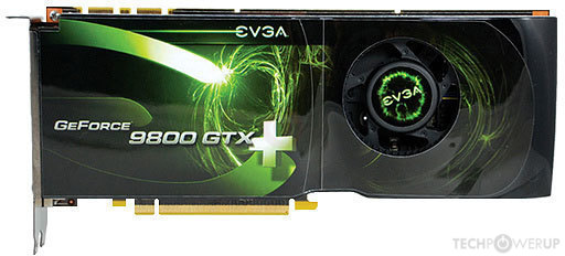
EVGA 9800 GTX+
- 512-P3-N873-AR
- 512-P3-N873-B2
- 512-P3-N873-FR
- 512-P3-N873-R1
- Graphics Processor
- G92B
- Cores
- 128
- TMUs
- 64
- ROPs
- 16
- Memory Size
- 512 MB
- Memory Type
- GDDR3
- Bus Width
- 256 bit

GPU
Graphics Processor
Graphics Card
- Release Date
- Jan 16th, 2009
- Generation
-
GeForce 9
(9800)
- Predecessor
- GeForce 8
- Successor
- GeForce 200
- Production
- End-of-life
- Bus Interface
- PCIe 2.0 x16
Clock Speeds
- GPU Clock
738 MHz
740 MHz
- Shader Clock
- 1836 MHz
- Memory Clock
-
1100 MHz
2.2 Gbps effective
Memory
- Memory Size
- 512 MB
- Memory Type
- GDDR3
- Memory Bus
- 256 bit
- Bandwidth
- 70.40 GB/s
Render Config
- Shading Units
- 128
- TMUs
- 64
- ROPs
- 16
- SM Count
- 16
- L2 Cache
- 64 KB
Theoretical Performance
- Pixel Rate
-
11.81 GPixel/s
11.84 GPixel/s
- Texture Rate
-
47.23 GTexel/s
47.36 GTexel/s
- FP32 (float)
- 470.0 GFLOPS
Board Design
- Slot Width
- Dual-slot
- Length
- 267 mm
10.5 inches
- Width
- 111 mm
4.4 inches
- Height
- 38 mm
1.5 inches
- TDP
- 141 W
- Suggested PSU
- 300 W
- Outputs
2x DVI
1x S-Video
2x DVI
1x HDMI
- Power Connectors
- 2x 6-pin
- Board Number
- P391 SKU 50,
P391 SKU 51,
P392 SKU 51,
P393 SKU 54
Graphics Features
- DirectX
- 11.1 (10_0)
- OpenGL
- 3.3
- OpenCL
- 1.1
- Vulkan
- N/A
- CUDA
- 1.1
- Shader Model
- 4.0
G92B GPU Notes
| PureVideo HD: VP2 VDPAU: Feature Set A |
Other retail boards based on this design (15)
| Name | GPU Clock | Memory Clock | Other Changes |
|---|---|---|---|
| 740 MHz | 1200 MHz | 254 mm/10 inches | |
| 775 MHz | 1180 MHz | ||
|
EVGA 9800 GTX+

|
740 MHz | 1100 MHz | 2x DVI 1x HDMI |
| 778 MHz | 1123 MHz | 2x DVI 1x HDMI | |
| 792 MHz | 1152 MHz | 2x DVI 1x HDMI | |
| 778 MHz | 1128 MHz | 2x DVI 1x HDMI | |
| 756 MHz | 1123 MHz | 241 mm/9.5 inches, 2x DVI 1x HDMI | |
| 738 MHz | 1100 MHz | 241 mm/9.5 inches, 2x DVI 1x HDMI | |
| 738 MHz | 1000 MHz | 1024 MB, 241 mm/9.5 inches | |
| 745 MHz | 1100 MHz | ||
| 760 MHz | 1150 MHz | ||
| 785 MHz | 1150 MHz | ||
| 775 MHz | 1125 MHz | ||
| 750 MHz | 1150 MHz | ||
| 750 MHz | 1150 MHz |


Apr 16th, 2024 00:16 EDT
change timezone
Latest GPU Drivers
New Forum Posts
- Is it possible that the atmosphere is losing less of its "shield" capabilities due to more and more jets/rockets puncturing it daily? (6)
- Cyberpunk 2077 Game Discussion (2113)
- Dell Workstation Owners Club (3046)
- Outer Worlds getting boring (4)
- Strange behaviour with my i5 1235u HP laptop after Windows reinstall (2)
- FINAL FANTASY XIV: Dawntrail Official Benchmark (27)
- Battery swap for cyberpower UPS (36)
- New pc old gpu intense mouse lag in every aspect (83)
- Your PC ATM (34464)
- Beware: Win11 KB5035853 Cumulative Update may cause stuttering and other performance problems. (12)
Popular Reviews
- Horizon Forbidden West Performance Benchmark Review - 30 GPUs Tested
- PowerColor Radeon RX 7900 GRE Hellhound Review
- Galax GeForce RTX 4070 Super EX Review
- Fractal Design Terra Review
- ASUS GeForce RTX 4090 Matrix Platinum Review - The RTX 4090 Ti
- Corsair 2000D Airflow Review
- Minisforum EliteMini UM780 XTX (AMD Ryzen 7 7840HS) Review
- Creative Pebble X Plus Review
- FiiO KB3 HiFi Mechanical Keyboard Review - Integrated DAC/Amp!
- ASUS GeForce RTX 4090 STRIX OC Review
Controversial News Posts
- NVIDIA Points Intel Raptor Lake CPU Users to Get Help from Intel Amid System Instability Issues (102)
- US Government Wants Nuclear Plants to Offload AI Data Center Expansion (98)
- Developers of Outpost Infinity Siege Recommend Underclocking i9-13900K and i9-14900K for Stability on Machines with RTX 4090 (82)
- Sony PlayStation 5 Pro Specifications Confirmed, Console Arrives Before Holidays (80)
- Windows 10 Security Updates to Cost $61 After 2025, $427 by 2028 (79)
- TechPowerUp Hiring: Reviewers Wanted for Motherboards, Laptops, Gaming Handhelds and Prebuilt Desktops (70)
- Intel Realizes the Only Way to Save x86 is to Democratize it, Reopens x86 IP Licensing (70)
- AMD Zen 5 Execution Engine Leaked, Features True 512-bit FPU (63)