Report an Error


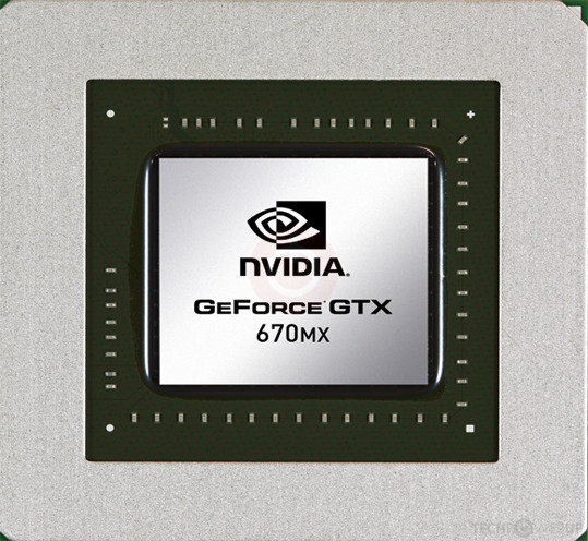
CLEVO GTX 670MX
- Graphics Processor
- GK104
- Cores
- 960
- TMUs
- 80
- ROPs
- 24
- Memory Size
- 3 GB
- Memory Type
- GDDR5
- Bus Width
- 192 bit

GPU
Graphics Processor
Mobile Graphics
- Release Date
- Oct 1st, 2012
- Generation
- GeForce 600M
- Predecessor
- GeForce 500M
- Successor
- GeForce 700M
- Production
- End-of-life
- Bus Interface
- PCIe 3.0 x16
Clock Speeds
- Base Clock
- 601 MHz
- Boost Clock
- 601 MHz
- Memory Clock
-
700 MHz
2.8 Gbps effective
Memory
- Memory Size
- 3 GB
- Memory Type
- GDDR5
- Memory Bus
- 192 bit
- Bandwidth
- 67.20 GB/s
Render Config
- Shading Units
- 960
- TMUs
- 80
- ROPs
- 24
- SMX Count
- 5
- L1 Cache
- 16 KB (per SMX)
- L2 Cache
- 384 KB
Theoretical Performance
- Pixel Rate
- 12.02 GPixel/s
- Texture Rate
- 48.08 GTexel/s
- FP32 (float)
- 1,154 GFLOPS
- FP64 (double)
- 48.08 GFLOPS (1:24)
Board Design
- TDP
- 75 W
- Outputs
- Portable Device Dependent
- Power Connectors
- None
Graphics Features
- DirectX
- 12 (11_0)
- OpenGL
- 4.6
- OpenCL
- 3.0
- Vulkan
- 1.2.175
- CUDA
- 3.0
- Shader Model
- 6.5 (5.1)
GK104 GPU Notes
| NVENC: 1st Gen NVDEC: 1st Gen PureVideo HD: VP5 VDPAU: Feature Set D L1 Cache is configurable from 16 KB up to 48 KB per SMX |
Other retail boards based on this design (2)
| Name | GPU Clock | Boost Clock | Memory Clock | Other Changes |
|---|---|---|---|---|
|
CLEVO GTX 670MX

|
601 MHz | 601 MHz | 700 MHz | |
| 615 MHz | 615 MHz | 700 MHz |

Apr 24th, 2024 12:05 EDT
change timezone
Latest GPU Drivers
New Forum Posts
- Is It The 1080 TI The Best GPU Ever? (207)
- What phone you use as your daily driver? And, a discussion of them. (1467)
- Cinebench crashed my PC. My Wi-Fi stopped working, and I keep getting a "Please wait" screen when I boot up my PC. (27)
- How are MX330 and İ5 1135G7 ? (1)
- AAF Optimus DCH Audio Modded Driver for Windows 10/11 - For ALL HDAUDIO Enumerator Chips (651)
- Realtek Modded Audio Driver for Windows 10/11 - Only for HDAUDIO (5689)
- Is there a technical reason that Windows 11 doesn't have built into it battery charge limitation? (39)
- EK seems to be having major issues (45)
- Looking to build another system (7)
- Which new games will you be buying? (311)
Popular Reviews
- Fractal Design Terra Review
- Thermalright Phantom Spirit 120 EVO Review
- Corsair 2000D Airflow Review
- Minisforum EliteMini UM780 XTX (AMD Ryzen 7 7840HS) Review
- ASUS GeForce RTX 4090 STRIX OC Review
- NVIDIA GeForce RTX 4090 Founders Edition Review - Impressive Performance
- ASUS GeForce RTX 4090 Matrix Platinum Review - The RTX 4090 Ti
- MSI GeForce RTX 4090 Gaming X Trio Review
- MSI GeForce RTX 4090 Suprim X Review
- Gigabyte GeForce RTX 4090 Gaming OC Review
Controversial News Posts
- Sony PlayStation 5 Pro Specifications Confirmed, Console Arrives Before Holidays (116)
- NVIDIA Points Intel Raptor Lake CPU Users to Get Help from Intel Amid System Instability Issues (106)
- AMD "Strix Halo" Zen 5 Mobile Processor Pictured: Chiplet-based, Uses 256-bit LPDDR5X (101)
- US Government Wants Nuclear Plants to Offload AI Data Center Expansion (98)
- Windows 10 Security Updates to Cost $61 After 2025, $427 by 2028 (84)
- Developers of Outpost Infinity Siege Recommend Underclocking i9-13900K and i9-14900K for Stability on Machines with RTX 4090 (84)
- TechPowerUp Hiring: Reviewers Wanted for Motherboards, Laptops, Gaming Handhelds and Prebuilt Desktops (78)
- Intel Realizes the Only Way to Save x86 is to Democratize it, Reopens x86 IP Licensing (70)