Report an Error


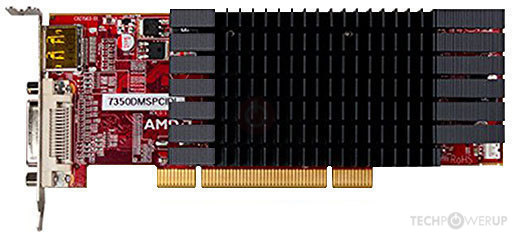
VisionTek HD 7350 PCI
- 900608
- Graphics Processor
- Cedar
- Cores
- 80
- TMUs
- 8
- ROPs
- 4
- Memory Size
- 512 MB
- Memory Type
- GDDR3
- Bus Width
- 64 bit
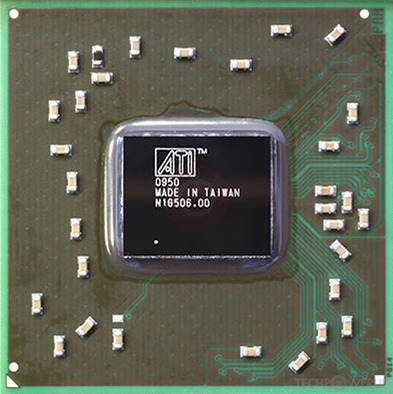
GPU
Graphics Processor
- GPU Name
- Cedar
- Architecture
- TeraScale 2
- Foundry
- TSMC
- Process Size
- 40 nm
- Transistors
- 292 million
- Density
- 4.9M / mm²
- Die Size
- 59 mm²
- Chip Package
- FCBGA-631
Graphics Card
- Release Date
- Jan 5th, 2012
- Generation
-
Southern Islands
(HD 7300)
- Predecessor
- Northern Islands
- Successor
- Sea Islands
- Production
- End-of-life
- Bus Interface
- PCI
Clock Speeds
- GPU Clock
- 650 MHz
- Memory Clock
-
500 MHz
533 MHz (+7%)
1000 Mbps effective
1066 Mbps effective
Memory
- Memory Size
- 512 MB
- Memory Type
- GDDR3
- Memory Bus
- 64 bit
- Bandwidth
-
8.000 GB/s
8.528 GB/s
Render Config
- Shading Units
- 80
- TMUs
- 8
- ROPs
- 4
- Compute Units
- 2
- L1 Cache
- 8 KB (per CU)
- L2 Cache
- 128 KB
Theoretical Performance
- Pixel Rate
- 2.600 GPixel/s
- Texture Rate
- 5.200 GTexel/s
- FP32 (float)
- 104.0 GFLOPS
Board Design
- Slot Width
- Single-slot
- TDP
- 19 W
- Suggested PSU
- 200 W
- Outputs
1x DVI
1x HDMI 1.3a
1x DVI
1x DisplayPort 1.1
Graphics Features
- DirectX
- 11.2 (11_0)
- OpenGL
- 4.4
- OpenCL
- 1.2
- Vulkan
- N/A
- Shader Model
- 5.0
Card Notes
| Rebranded HD 5450/6350 |
Cedar GPU Notes
| Generation: Evergreen Mobile Variant: Park / Robson Graphics/Compute: GFX4 Display Core Engine: 4.0 Unified Video Decoder: 2.3 |
Other retail boards based on this design (1)
| Name | GPU Clock | Memory Clock | Other Changes |
|---|---|---|---|
|
VisionTek HD 7350 PCI

|
650 MHz | 533 MHz | 1x DVI 1x DisplayPort |
Apr 24th, 2024 14:04 EDT
change timezone
Latest GPU Drivers
New Forum Posts
- How are MX330 and İ5 1135G7 ? (6)
- Realtek Modded Audio Driver for Windows 10/11 - Only for HDAUDIO (5690)
- I7-8750H + GTX 1050ti Laptop drops performance periodically (5)
- Aida64 cache mem OC (6)
- Official Board Game Discussion (20)
- Rare GPUs / Unreleased GPUs (1873)
- !BEWARE! ASRock B650E Steel Legend CPU Destroying Bios BUG! (60)
- need help with motherboard/ ram compability certainty (16)
- Which new games will you be buying? (312)
- Meta Horizon OS (11)
Popular Reviews
- Fractal Design Terra Review
- Thermalright Phantom Spirit 120 EVO Review
- Corsair 2000D Airflow Review
- Minisforum EliteMini UM780 XTX (AMD Ryzen 7 7840HS) Review
- ASUS GeForce RTX 4090 STRIX OC Review
- NVIDIA GeForce RTX 4090 Founders Edition Review - Impressive Performance
- ASUS GeForce RTX 4090 Matrix Platinum Review - The RTX 4090 Ti
- MSI GeForce RTX 4090 Suprim X Review
- MSI GeForce RTX 4090 Gaming X Trio Review
- Gigabyte GeForce RTX 4090 Gaming OC Review
Controversial News Posts
- Sony PlayStation 5 Pro Specifications Confirmed, Console Arrives Before Holidays (116)
- NVIDIA Points Intel Raptor Lake CPU Users to Get Help from Intel Amid System Instability Issues (106)
- AMD "Strix Halo" Zen 5 Mobile Processor Pictured: Chiplet-based, Uses 256-bit LPDDR5X (101)
- US Government Wants Nuclear Plants to Offload AI Data Center Expansion (98)
- Windows 10 Security Updates to Cost $61 After 2025, $427 by 2028 (84)
- Developers of Outpost Infinity Siege Recommend Underclocking i9-13900K and i9-14900K for Stability on Machines with RTX 4090 (84)
- TechPowerUp Hiring: Reviewers Wanted for Motherboards, Laptops, Gaming Handhelds and Prebuilt Desktops (78)
- Intel Realizes the Only Way to Save x86 is to Democratize it, Reopens x86 IP Licensing (70)