Report an Error


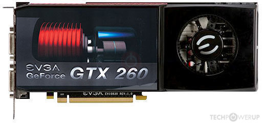
EVGA GTX 260 Core 216 Superclocked
- 896-P3-1257-AR
- 896-P3-1257-ER
- Graphics Processor
- GT200B
- Cores
- 216
- TMUs
- 72
- ROPs
- 28
- Memory Size
- 896 MB
- Memory Type
- GDDR3
- Bus Width
- 448 bit
GPU
Graphics Processor
Graphics Card
- Release Date
Nov 27th, 2008
Dec 2nd, 2008
- Generation
- GeForce 200
- Predecessor
- GeForce 9
- Successor
- GeForce 400
- Production
- End-of-life
- Bus Interface
- PCIe 2.0 x16
Clock Speeds
- GPU Clock
576 MHz
626 MHz (+9%)
- Shader Clock
1242 MHz
1350 MHz (+9%)
- Memory Clock
-
999 MHz
1053 MHz (+5%)
1998 Mbps effective
2.1 Gbps effective
Memory
- Memory Size
- 896 MB
- Memory Type
- GDDR3
- Memory Bus
- 448 bit
- Bandwidth
-
111.9 GB/s
117.9 GB/s
Render Config
- Shading Units
- 216
- TMUs
- 72
- ROPs
- 28
- SM Count
- 27
- L2 Cache
- 224 KB
Theoretical Performance
- Pixel Rate
-
16.13 GPixel/s
17.53 GPixel/s
- Texture Rate
-
41.47 GTexel/s
45.07 GTexel/s
- FP32 (float)
-
536.5 GFLOPS
583.2 GFLOPS
- FP64 (double)
-
67.07 GFLOPS
72.90 GFLOPS (1:8)
Board Design
- Slot Width
- Dual-slot
- TDP
- 171 W
- Suggested PSU
- 450 W
- Outputs
- 2x DVI
1x S-Video
- Power Connectors
- 2x 6-pin
- Board Number
- P654 SKU 51,
P897 SKU 53,
P897 SKU 54
Graphics Features
- DirectX
- 11.1 (10_0)
- OpenGL
- 3.3
- OpenCL
- 1.1
- Vulkan
- N/A
- CUDA
- 1.3
- Shader Model
- 4.0
GT200B GPU Notes
| PureVideo HD: VP2 VDPAU: Feature Set A GT200B, commonly printed on the chip package as G200-xxx-Bx is an optical shrink of the G200 core to the newer 55 manufacturing process of TSMC. It helped shrink the core's energy and thermal footprints to a level that even facilitated building a dual-GPU accelerator |
Other retail boards based on this design (18)
| Name | GPU Clock | Memory Clock | Other Changes |
|---|---|---|---|
| 576 MHz | 1015 MHz | ||
| 576 MHz | 999 MHz | ||
| 576 MHz | 999 MHz | ||
| 675 MHz | 1151 MHz | ||
|
EVGA GTX 260 Core 216 Superclocked

|
626 MHz | 1053 MHz | |
| 585 MHz | 999 MHz | 270 mm/10.6 inches, 1x DVI 1x HDMI 1x VGA | |
| 650 MHz | 1200 MHz | 1792 MB, 270 mm/10.6 inches | |
| 650 MHz | 999 MHz | 1x DVI 1x HDMI 1x VGA | |
| 680 MHz | 1250 MHz | 1x DVI 1x HDMI 1x VGA | |
| 576 MHz | 999 MHz | ||
| 680 MHz | 1050 MHz | 1792 MB, 1x DVI 1x HDMI 1x VGA | |
| 655 MHz | 999 MHz | 1792 MB, 1x DVI 1x HDMI 1x VGA | |
| 576 MHz | 999 MHz | ||
| 625 MHz | 1100 MHz | ||
| 576 MHz | 1000 MHz | 229 mm/9 inches, 1x DVI 1x HDMI 1x VGA | |
| 576 MHz | 999 MHz | ||
| 650 MHz | 1050 MHz | ||
| 650 MHz | 1050 MHz | 2x DVI |


Apr 18th, 2024 08:30 EDT
change timezone
Latest GPU Drivers
New Forum Posts
- What's your latest tech purchase? (20254)
- Will a RTX 4070 TI super bottleneck a Ryzen 9 7950X3D? (33)
- Which air cooler for a ryzen 9 5900x (157)
- What are you playing? (20454)
- Unlocked Realtek HD Audio Drivers for Windows 11 (Dolby Digital Live/DTS Interactive) (152)
- The TPU UK Clubhouse (24726)
- Gigabyte gpu model differences? (33)
- DDR5 RAM Speeds and the future (25)
- [Official] Meta Quest 3 (43)
- Realtek Modded Audio Driver for Windows 10/11 - Only for HDAUDIO (5677)
Popular Reviews
- Horizon Forbidden West Performance Benchmark Review - 30 GPUs Tested
- PowerColor Radeon RX 7900 GRE Hellhound Review
- Fractal Design Terra Review
- Corsair 2000D Airflow Review
- Minisforum EliteMini UM780 XTX (AMD Ryzen 7 7840HS) Review
- Creative Pebble X Plus Review
- FiiO KB3 HiFi Mechanical Keyboard Review - Integrated DAC/Amp!
- ASUS GeForce RTX 4090 STRIX OC Review
- NVIDIA GeForce RTX 4090 Founders Edition Review - Impressive Performance
- ASUS GeForce RTX 4090 Matrix Platinum Review - The RTX 4090 Ti
Controversial News Posts
- Sony PlayStation 5 Pro Specifications Confirmed, Console Arrives Before Holidays (106)
- NVIDIA Points Intel Raptor Lake CPU Users to Get Help from Intel Amid System Instability Issues (102)
- US Government Wants Nuclear Plants to Offload AI Data Center Expansion (98)
- Windows 10 Security Updates to Cost $61 After 2025, $427 by 2028 (82)
- Developers of Outpost Infinity Siege Recommend Underclocking i9-13900K and i9-14900K for Stability on Machines with RTX 4090 (82)
- TechPowerUp Hiring: Reviewers Wanted for Motherboards, Laptops, Gaming Handhelds and Prebuilt Desktops (71)
- Intel Realizes the Only Way to Save x86 is to Democratize it, Reopens x86 IP Licensing (70)
- AMD Zen 5 Execution Engine Leaked, Features True 512-bit FPU (63)