Report an Error


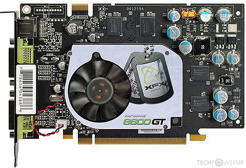
XFX 8600 GT XXX Edition
- PVT84JUDD3
- Graphics Processor
- G84
- Cores
- 32
- TMUs
- 16
- ROPs
- 8
- Memory Size
- 256 MB
- Memory Type
- GDDR3
- Bus Width
- 128 bit

GPU
Graphics Processor
Graphics Card
- Release Date
Apr 17th, 2007
Jun 11th, 2007
- Generation
-
GeForce 8
(8600)
- Predecessor
- GeForce 7 PCIe
- Successor
- GeForce 9
- Production
- End-of-life
- Bus Interface
- PCIe 1.0 x16
Clock Speeds
- GPU Clock
540 MHz
620 MHz (+15%)
- Shader Clock
1190 MHz
1457 MHz (+22%)
- Memory Clock
-
700 MHz
800 MHz (+14%)
1400 Mbps effective
1600 Mbps effective
Memory
- Memory Size
-
512 MB
256 MB
- Memory Type
- GDDR3
- Memory Bus
- 128 bit
- Bandwidth
-
22.40 GB/s
25.60 GB/s
Render Config
- Shading Units
- 32
- TMUs
- 16
- ROPs
- 8
- SM Count
- 4
- L2 Cache
- 32 KB
Theoretical Performance
- Pixel Rate
-
4.320 GPixel/s
4.960 GPixel/s
- Texture Rate
-
8.640 GTexel/s
9.920 GTexel/s
- FP32 (float)
-
76.16 GFLOPS
93.25 GFLOPS
Board Design
- Slot Width
- Single-slot
- TDP
- 47 W
- Suggested PSU
- 200 W
- Outputs
- 2x DVI
1x S-Video
- Power Connectors
- None
- Board Number
- P402,
P403 SKU 6
Graphics Features
- DirectX
- 11.1 (10_0)
- OpenGL
- 3.3
- OpenCL
- 1.1
- Vulkan
- N/A
- CUDA
- 1.1
- Shader Model
- 4.0
Card Notes
| Memory Variant: 1 GB |
G84 GPU Notes
| PureVideo HD: VP2 VDPAU: Feature Set A |
Other retail boards based on this design (4)
| Name | GPU Clock | Memory Clock | Other Changes |
|---|---|---|---|
| 540 MHz | 800 MHz | DDR2, 1x DVI 1x VGA 1x S-Video | |
| 540 MHz | 700 MHz | 256 MB | |
|
XFX 8600 GT XXX Edition

|
620 MHz | 800 MHz | 256 MB |
| 600 MHz | 800 MHz | 161 mm/6.3 inches |


Apr 23rd, 2024 10:09 EDT
change timezone
Latest GPU Drivers
New Forum Posts
- Windows 12 (142)
- Possible near-future 2024 Arrow Lake build.... (48)
- EK seems to be having major issues (25)
- Odd RTX 3080 behaviour (2)
- Show us your collections thread!! (281)
- Serious bug in PHP reported! (2)
- Upgrade Build (105)
- The Official Linux/Unix Desktop Screenshots Megathread (693)
- Share your AIDA 64 cache and memory benchmark here (2913)
- My computer setup - Request for opinions (4)
Popular Reviews
- Horizon Forbidden West Performance Benchmark Review - 30 GPUs Tested
- Fractal Design Terra Review
- Corsair 2000D Airflow Review
- Thermalright Phantom Spirit 120 EVO Review
- Minisforum EliteMini UM780 XTX (AMD Ryzen 7 7840HS) Review
- ASUS GeForce RTX 4090 STRIX OC Review
- NVIDIA GeForce RTX 4090 Founders Edition Review - Impressive Performance
- ASUS GeForce RTX 4090 Matrix Platinum Review - The RTX 4090 Ti
- Creative Pebble X Plus Review
- MSI GeForce RTX 4090 Gaming X Trio Review
Controversial News Posts
- Sony PlayStation 5 Pro Specifications Confirmed, Console Arrives Before Holidays (116)
- NVIDIA Points Intel Raptor Lake CPU Users to Get Help from Intel Amid System Instability Issues (105)
- AMD "Strix Halo" Zen 5 Mobile Processor Pictured: Chiplet-based, Uses 256-bit LPDDR5X (101)
- US Government Wants Nuclear Plants to Offload AI Data Center Expansion (98)
- Windows 10 Security Updates to Cost $61 After 2025, $427 by 2028 (84)
- Developers of Outpost Infinity Siege Recommend Underclocking i9-13900K and i9-14900K for Stability on Machines with RTX 4090 (82)
- TechPowerUp Hiring: Reviewers Wanted for Motherboards, Laptops, Gaming Handhelds and Prebuilt Desktops (74)
- Intel Realizes the Only Way to Save x86 is to Democratize it, Reopens x86 IP Licensing (70)