News Posts matching #10 nm

Return to Keyword Browsing

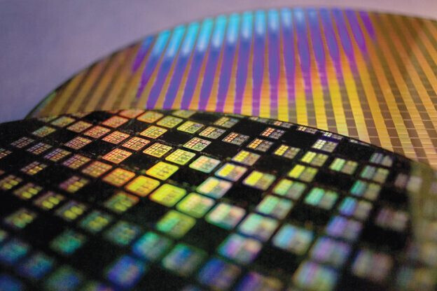
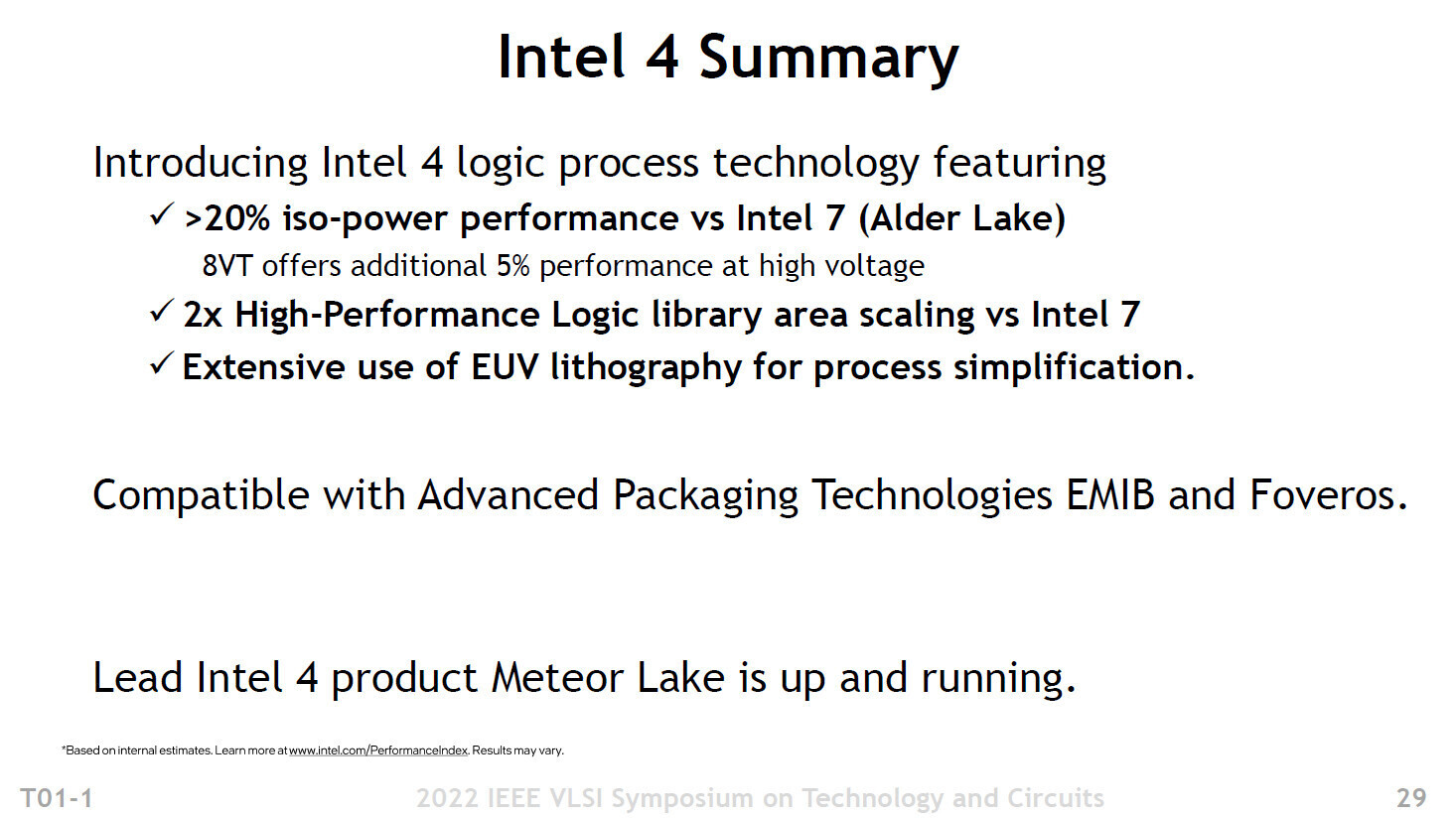
Huawei and SMIC Prepare Quadruple Semiconductor Patterning for 5 nm Production

According to Bloomberg's latest investigation, Huawei and Semiconductor Manufacturing International Corporation (SMIC) have submitted patents on the self-aligned quadruple patterning (SAQP) pattern etching technique to enable SMIC to achieve 5 nm semiconductor production. The two Chinese giants have been working with the Deep Ultra Violet (DUV) machinery to develop a pattern etching technique allowing SMIC to produce a node compliant with the US exporting rules while maintaining the density improvements from the previously announced 7 nm node. In the 7 nm process, SMIC most likely used self-aligned dual patterning (SADP) with DUV tools, but for the increased density of the 5 nm node, a doubling to SAQP is required. In semiconductor manufacturing, lithography tools take multiple turns to etch the design of the silicon wafer.

Especially with smaller nodes getting ever-increasing density requirements, it is becoming challenging to etch sub-10 nm designs using DUV tools. That is where Extreme Ultra Violet (EUV) tools from ASML come into play. With EUV, the wavelengths of the lithography printers are 14 times smaller than DUV, at only 13.5 nm, compared to 193 nm of ArF immersion DUV systems. This means that without EUV, SMIC has to look into alternatives like SAQP to increase the density of its nodes and, as a result, include more complications and possibly lower yields. As an example, Intel tried to use SAQP in its first 10 nm nodes to reduce reliance on EUV, which resulted in a series of delays and complications, eventually pushing Intel into EUV. While Huawei and SMIC may develop a more efficient solution for SAQP, the use of EUV is imminent as the regular DUV can not keep up with the increasing density of semiconductor nodes. Given that ASML can't ship its EUV machinery to China, Huawei is supposedly developing its own EUV machines, but will likely take a few more years to show.

Samsung to Also Showcase 280-layer 3D QLC NAND Flash, 32 Gbit DDR5-8000 Memory Chips at IEEE-SSCC

In addition to the 37 Gbps GDDR7 memory, Samsung Electronics prepares to showcase several other memory innovations at the 2024 IEEE-SSCC as compiled by VideoCardz. To begin with, the company is showcasing a new 280-layer 3D QLC NAND flash memory in the 1 Tb density, enabling next generation of mainstream SSDs and smartphone storage. This chip offers an areal density of 28.5 Gb/mm², and a speed of 3.2 GB/s. To put this into perspective, the fastest 3D NAND flash types powering the current crop of flagship NVMe SSDs rely on 2.4 GB/s of I/O data rates.

Next up, is a new generation DDR5 memory chip offers data rates of DDR5-8000 with a density of 32 Gbit (4 GB). This chip uses a symmetric-mosaic DRAM cell architecture, and is built on a 5th generation 10 nm class foundry node Samsung optimized for DRAM products. What's impressive about this chip is that it will allow PC memory vendors to build 32 GB and 48 GB DIMMs in single-rank configuration with DDR5-8000 speeds; as well as 64 GB and 96 GB DIMMs in dual-rank configuration (impressive, provided your platform can play well with DDR5-8000 in dual-rank).

Ayar Labs Showcases 4 Tbps Optically-enabled Intel FPGA at Supercomputing 2023

Ayar Labs, a leader in silicon photonics for chip-to-chip connectivity, will showcase its in-package optical I/O solution integrated with Intel's industry-leading Agilex Field-Programmable Gate Array (FPGA) technology. In demonstrating 5x current industry bandwidth at 5x lower power and 20x lower latency, the optical FPGA - packaged in a common PCIe card form factor - has the potential to transform the high performance computing (HPC) landscape for data-intensive workloads such as generative artificial intelligence (AI), machine learning, and support novel new disaggregated compute and memory architectures and more.

"We're on the cusp of a new era in high performance computing as optical I/O becomes a 'must have' building block for meeting the exponentially growing, data-intensive demands of emerging technologies like generative AI," said Charles Wuischpard, CEO of Ayar Labs. "Showcasing the integration of Ayar Labs' silicon photonics and Intel's cutting-edge FPGA technology at Supercomputing is a concrete demonstration that optical I/O has the maturity and manufacturability needed to meet these critical demands."

WEROCK Presents the New Rocksmart RSC612 Industrial Panel PC

WEROCK Technologies GmbH, innovative manufacturer of industrial computer technology, continues its innovative Rocksmart model series and introduces the latest member: the Rocksmart RSC612. The powerful industrial panel PC builds on the success of the Rocksmart RSC610 and expands the possibilities for machine and plant construction as well as the automation industry.

The demands placed on modern technological applications are constantly increasing. The new Rocksmart RSC612 Industrial Panel PC has been specially developed to meet these requirements and offers a wide range of functions. Like the recently introduced Rocksmart RSC610, the new model offers a slim aluminium housing for a modern aesthetic and IP65 protection on the front. The completely passive cooling and the wide operating temperature range ensure a wide range of applications. The Panel PC can be mounted in control cabinets or positioned anywhere thanks to VESA mounting points.

SK hynix Presents Advanced Memory Technologies at Intel Innovation 2023

SK hynix announced on September 22 that it showcased its latest memory technologies and products at Intel Innovation 2023 held September 19-20 in the western U.S. city of San Jose, California. Hosted by Intel since 2019, Intel Innovation is an annual IT exhibition which brings together the technology company's customers and partners to share the latest developments in the industry. At this year's event held at the San Jose McEnery Convention Center, SK hynix showcased its advanced semiconductor memory products which are essential in the generative AI era under the slogan "Pioneer Tomorrow With the Best."

Products that garnered the most interest were HBM3, which supports the high-speed performance of AI accelerators, and DDR5 RDIMM, a DRAM module for servers with 1bnm process technology. As one of SK hynix's core technologies, HBM3 has established the company as a trailblazer in AI memory. SK hynix plans to further strengthen its position in the market by mass-producing HBM3E (Extended) from 2024. Meanwhile, DDR5 RDIMM with 1bnm, or the 5th generation of the 10 nm process technology, also offers outstanding performance. In addition to supporting unprecedented transfer speeds of more than 6,400 megabits per second (Mbps), this low-power product helps customers simultaneously reduce costs and improve ESG performance.

SK hynix Reports Second Quarter 2023 Financial Results

SK hynix Inc. today reported financial results for the second quarter of 2023. The company recorded revenue of 7.306 trillion won, operating loss of 2.882 trillion won (with operating margin of negative 39%), and net loss of 2.988 trillion won (with net margin of negative 41%) for the three-month period ended June 30, 2023.

"Amid an expansion in generative artificial intelligence (AI) market, which has largely been centered on ChatGPT, demand for AI server memory has increased rapidly," the company said. "As a result, sales of premium products such as HBM3 and DDR5 increased, leading to a 44% sequential increase in revenue for the second quarter, while operating loss narrowed by 15%."

SK hynix Enters Industry's First Compatibility Validation Process for 1bnm DDR5 Server DRAM

SK hynix Inc. announced today that it has completed the development of the industry's most advanced 1bnm, the fifth-generation of the 10 nm process technology, while the company and Intel began a joint evaluation of 1bnm and validation in the Intel Data Center Certified memory program for DDR5 products targeted at Intel Xeon Scalable platforms.

The move comes after SK hynix became the first in the industry to reach 1anm readiness and completed Intel's system validation of the 1anm DDR5, the fourth-generation of the 10 nm technology. The DDR5 products provided to Intel run at the world's fastest speed of 6.4 Gbps (Gigabits per second), representing a 33% improvement in data processing speed compared with test-run products in early days of DDR5 development.

Intel "Emerald Rapids" Doubles Down on On-die Caches, Divests on Chiplets

Finding itself embattled with AMD's EPYC "Genoa" processors, Intel is giving its 4th Gen Xeon Scalable "Sapphire Rapids" processor a rather quick succession in the form of the Xeon Scalable "Emerald Rapids," bound for Q4-2023 (about 8-10 months in). The new processor shares the same LGA4677 platform and infrastructure, and much of the same I/O, but brings about two key design changes that should help Intel shore up per-core performance, making it competitive to EPYC "Zen 4" processors with higher core-counts. SemiAnalysis compiled a nice overview of the changes, the two broadest points of it being—1. Intel is peddling back on the chiplet approach to high core-count CPUs, and 2., that it wants to give the memory sub-system and inter-core performance a massive performance boost using larger on-die caches.

The "Emerald Rapids" processor has just two large dies in its extreme core-count (XCC) avatar, compared to "Sapphire Rapids," which can have up to four of these. There are just three EMIB dies interconnecting these two, compared to "Sapphire Rapids," which needs as many as 10 of these to ensure direct paths among the four dies. The CPU core count itself doesn't see a notable increase. Each of the two dies on "Emerald Rapids" physically features 33 CPU cores, so a total of 66 are physically present, although one core per die is left unused for harvesting, the SemiAnalysis article notes. So the maximum core-count possible commercially is 32 cores per die, or 64 cores per socket. "Emerald Rapids" continues to be based on the Intel 7 process (10 nm Enhanced SuperFin), probably with a few architectural improvements for higher clock-speeds.

SK Hynix Believes the Memory Chip Market Has Hit Rock Bottom

Yesterday SK Hynix reported its Q1 2023 results and to say that they were abysmal is being kind, as the company reported a 3.4 trillion won operating loss, or just over US$2.5 billion. That's no small hit to take for any company, especially when it's only the performance for a single quarter. However, SK Hynix is apparently trying to see its situation from a positive perspective and believes that the memory chip market will rebound in the second half of this year. The positive outlook isn't just based on what SK Hynix believes though, as various analysts and securities companies believe in an upswing in the second half of the year.

That said, Micron, one of SK Hynix main competitors, has a more drab outlook for the remainder of 2023 and is expecting a tough year ahead. SK Hynix is expecting production cuts by itself, Micron and Samsung to start to take effect sometime in the second quarter this year, which should see inventory drop to more normal levels for all three companies. SK Hynix is also expecting to see a higher demand for DDR5 DRAM later this year, especially in the mobile and server market space. Finally, SK Hynix is hoping that its customers will buy higher density memory products this year, replacing older, lower density solutions, be that DRAM or NAND flash related. SK Hynix is expecting to launch its Gen 5 10 nm DRAM and 238-layer NAND sometime next year, which the company is also hoping will bring more income to its coffers, but the company still has to make it through the rest of 2023 first.

SK hynix Develops LPDDR5T, World's Fastest Mobile DRAM

SK hynix Inc. announced today that it has developed the world's fastest mobile DRAM 'LPDDR5T (Low Power Double Data Rate 5 Turbo)' and provided sample products to customers. The new product, LPDDR5T, operates at a data rate of 9.6 gigabits per second (Gbps), 13% faster than the previous generation LPDDR5X unveiled in November 2022. To highlight the maximum speed the product features, SK hynix added 'Turbo' at the end of the standard name LPDDR5.

LPDDR5T, which operates in the ultra-low voltage range of 1.01 to 1.12 V set by the JEDEC (Joint Electron Device Engineering Council), is a product that not only features utmost speed but ultra-low power consumption. "The company pushed the technology to new limits in just two months after LPDDR5X, mobile DRAM with 8.5 Gbps specification, was introduced to the market in November 2022," SK hynix said. "We will solidify our leadership in the mobile DRAM market by providing products of various storage capacities that meet customers' needs."

SK hynix Obtains Industry's First Validation for 1anm DDR5 DRAM on the 4th Gen Intel Xeon Scalable Processor

SK hynix Inc. (or "the company", www.skhynix.com) announced today that its DDR5 product for servers using 1anm, the fourth generation of the 10 nm process technology, has been validated on the 4th Gen Intel Xeon Scalable processor (formerly codenamed Sapphire Rapids) for the first time in the industry. "The validation of the 1anm DDR5 compatibility by Intel for its newest processor that supports DDR5 for the first time is monumental," SK hynix said. "We will seek a fast turnaround in the semiconductor memory industry by actively responding to the growing server market through DDR5, which is already in mass production."

The validation of the company's 1anm DDR5 product, which adopts 1anm technology using the EUV lithography process, is for 4th Gen Intel Xeon Scalable processors, Intel's latest server CPU launched on January 10th. The 4th Gen Intel Xeon Scalable processor has been cited as a key to a turnaround in the industry, given that the launch of a next-generation server CPU requires server replacement and thus, results in a rapid increase in demand for high-performance memory chips. Experts predict that DDR5, expected to meet customers' such needs, will soon become the flagship product in the server DRAM market.

AMD Explains the Economics Behind Chiplets for GPUs

AMD, in its technical presentation for the new Radeon RX 7900 series "Navi 31" GPU, gave us an elaborate explanation on why it had to take the chiplets route for high-end GPUs, devices that are far more complex than CPUs. The company also enlightened us on what sets chiplet-based packages apart from classic multi-chip modules (MCMs). An MCM is a package that consists of multiple independent devices sharing a fiberglass substrate.

An example of an MCM would be a mobile Intel Core processor, in which the CPU die and the PCH die share a substrate. Here, the CPU and the PCH are independent pieces of silicon that can otherwise exist on their own packages (as they do on the desktop platform), but have been paired together on a single substrate to minimize PCB footprint, which is precious on a mobile platform. A chiplet-based device is one where a substrate is made up of multiple dies that cannot otherwise independently exist on their own packages without an impact on inter-die bandwidth or latency. They are essentially what should have been components on a monolithic die, but disintegrated into separate dies built on different semiconductor foundry nodes, with a purely cost-driven motive.

Samsung Electronics Envisions Hyper-Growth in Memory and Logic Semiconductors through Intensified Industry Collaborations

Samsung Electronics Co., Ltd., a world leader in advanced semiconductor technology, today showcased a series of cutting-edge semiconductor solutions set to drive digital transformation through the decade, at Samsung Tech Day 2022. An annual conference since 2017, the event returned to in-person attendance at the Signia by Hilton San Jose hotel after three years.

This year's event, attended by more than 800 customers and partners, featured presentations from Samsung's Memory and System LSI business leaders—including Jung-bae Lee, President and Head of Memory Business; Yong-In Park, President and Head of System LSI Business; and Jaeheon Jeong, Executive Vice President and Head of Device Solutions (DS) Americas Office—on the company's latest advancements and its vision for the future.

Intel "Raptor Lake" 8P+16E Wafer Pictured

Andreas Schilling with Hardwareluxx.de, as part of the Intel Tech Tour Israel, got to hold a 12-inch wafer full of "Raptor Lake-S" dies. These are dies in their full 8P+16E configuration. The die is estimated to measure 257 mm² in area. We count 231 full dies on this wafer. Intel is building "Raptor Lake" on the same 10 nm Enhanced SuperFin (aka Intel 7) node as "Alder Lake." The die is about 23% larger than "Alder Lake" on account of two additional E-core clusters, possibly larger P-cores, and larger L2 caches for both the P-core and E-core clusters. "Raptor Lake" gains significance as it will be the last client processor from Intel to be built on a monolithic die of a uniform silicon fabrication node. Future generations are expected to take the chiplets route, realizing the company's IDM 2.0 product development strategy.

Latency Increase from Larger L2 Cache on Intel "Raptor Cove" P-core Well Contained: Report

According to an investigative report by "Chips and Cheese," the larger L2 caches in Intel's 13th Gen Core "Raptor Lake-S" doesn't come with a proportionate increase in cache latency, and Intel seems to have contained the latency increase well. "Raptor Lake-S" significantly increases L2 cache sizes over the previous generation. Each of its 8 "Raptor Cove" P-cores has 2 MB of dedicated L2 cache, compared to the 1.25 MB with the "Golden Cove" P-cores powering the current-gen "Alder Lake-S," which amounts to a 60 percent increase in size. The "Gracemont" E-core clusters (group of four E-cores), sees a doubling in the size of the L2 cache that's shared among the four cores in the cluster, from 2 MB in "Alder Lake," to 4 MB. The last-level L3 cache shared among all P-cores and E-core clusters, sees a less remarkable increase in size, from 30 MB to 36 MB.

Larger caches have a direct impact on performance, as more data is available close to the CPU cores, sparing them a lengthy fetch/store operation to the main memory (RAM). However, making caches larger doesn't just cost die-area, transistor-count, and power/heat, but also latency, even though L2 cache is an order of magnitude faster than the L3 cache, which in turn is significantly faster than DRAM. Chips and Cheese tracked and tabulated the L2 cache latencies of past Intel client microarchitectures, and found a generational increase in latencies with increasing L2 cache sizes, leading up to "Alder Lake." This increase has somehow tapered with "Raptor Lake."

Intel "Raptor Lake" Core i9-13900 De-lidded, Reveals a 23% Larger Die than Alder Lake

An Intel Core "Raptor Lake" engineering sample was de-lidded by Expreview giving us a first look at what will be Intel's last monolithic silicon client processor before the company switches over to chiplets, with its next-generation "Meteor Lake." The chip de-lidded here is the i9-13900, which maxes out the "Raptor Lake-S" die, in featuring all 8 "Raptor Cove" P-cores and 16 "Gracemont" E-cores physically present on the die, along with 36 MB of shared L3 cache, and an iGPU based on the Xe-LP graphics architecture.

The "Raptor Lake-S" silicon is built on the same Intel 7 (10 nm Enhanced SuperFin) silicon fabrication node as "Alder Lake-S." The "Raptor Lake-S" (8P+16E) die measures 23.8 mm x 10.8 mm, or 257 mm² in area, which is 49 mm² more than that of the "Alder Lake-S" (8P+8E) die (around 209 mm²). The larger die area comes from not just the two additional E-core clusters, but also larger L2 caches for the E-core clusters (4 MB vs. 2 MB), and larger L2 caches for the P-cores (2 MB vs. 1.25 MB); besides the larger shared L3 cache (36 MB vs. 30 MB). The "Raptor Cove" P-core itself could be slightly larger than its "Golden Cove" predecessor.

Intel "Raptor Lake" Core i9 Sample Powers Up, 8P+16E Configuration Confirmed

An engineering sample of a 13th Intel Core "Raptor Lake" Core i9 processor hit the web, courtesy of wxnod on Twitter, which confirms its 8P+16E core-configuration in a CPU-Z screenshot. Based on the same LGA1700 package as "Alder Lake," and backwards compatible with Intel 600-series chipset motherboards, besides new 700-series ones, "Raptor Lake" combines eight "Raptor Cove" performance cores (P-cores), with sixteen "Gracemont" efficiency cores (E-cores).

"Raptor Cove" features a generational IPC increase over the "Golden Cove" P-cores powering "Alder Lake," while the "Gracemont" E-cores, although identical to those on "Alder Lake," are expected to benefit from the doubling in L2 cache per cluster, from 2 MB to 4 MB. The ISA as detected by CPU-Z appears to be identical to that of "Alder Lake." The processor is a monolithic silicon chip built on the Intel 7 (10 nm Enhanced SuperFin) silicon fabrication process.

Nanya Kicks Off Construction of US$10 Billion Fab in New Taipei City

Nanya Technology, part of the Formosa Plastics Group, which is one of the largest conglomerates in Taiwan, will hold a ground-breaking ceremony for its new 12-inch fab that will be built in New Taipei City later this week. It'll be the biggest investment Nanya has done in the past decade, as the company is investing US$10.1 billion into building the new fab. This is obviously a lot less than TSMC is investing, but DRAM is made on different nodes to those that TSMC makes its customers products on, since DRAM doesn't benefit as much from node shrinking as other types of semiconductors.

The new fab will be located near one of Nanya's current fabs, in the Taishan district. Mass production is scheduled to start some time in 2025 and the fab is said to have a monthly capacity of around 45,000 wafers. Right now it's scheduled for a 10 nm technology node, but this might change by the time that the fab is up and running, especially considering that Nanya is already producing a range of 10 nm based products in some of its current fabs. Nanya's goal is to develop its next generation of 10 nm DRAM independently from other DRAM makers, as to avoid having to pay patent licence fees to its competitors.

Intel 4 Process Node Detailed, Doubling Density with 20% Higher Performance

Intel's semiconductors nodes have been quite controversial with the arrival of the 10 nm design. Years in the making, the node got delayed multiple times, and only recently did the general public get the first 10 nm chips. Today, at IEEE's annual VLSI Symposium, we get more details about Intel's upcoming nodes, called Intel 4. Previously referred to as a 7 nm process, Intel 4 is the company's first node to use EUV lithography accompanied by various technologies. The first thing when a new process node is discussed is density. Compared to Intel 7, Intel 4 will double the transistor count for the same area and enable 20% higher performing transistors.

Looking at individual transistor size, the new Intel 4 node represents a very tiny piece of silicon that is even smaller than its predecessor. With a Fin Pitch of 30 nm, Contact Gate Poly Pitch of 50 nm between gates, and Minimum Metal Pitch (M0) of 50 nm, the Intel 4 transistor is significantly smaller compared to the Intel 7 cell, listed in the table below. For scaling, Intel 4 provides double the number of transistors in the same area compared to Intel 7. However, this reasoning is applied only to logic. For SRAM, the new PDK provides 0.77 area reduction, meaning that the same SoC built on Intel 7 will not be half the size of Intel 4, as SRAM plays a significant role in chip design. The Intel 7 HP library can put 80 million transistors on a square millimeter, while Intel 4 HP is capable of 160 million transistors per square millimeter.

GIGABYTE Announces the BRIX Extreme, the Most Powerful Mini PC in the World

GIGABYTE Technology, a leading manufacturer of motherboards, graphics cards, and hardware solutions, today announced the all-new 2022 BRIX Extreme mini-PC series, which adopts the latest 12th Gen Intel Core Mobile Processors with Intel's most scalable client architecture that delivers superior computing performance. Benefiting from a new Intel Core design for leadership performance, these processors boost the performance significantly in the all-new performance hybrid design for superior single-threaded & multi-threaded performance. Enhanced by GIGABYTE's exclusive design, the new 2022 BRIX Extreme design integrates four display outputs, including HDMI 2.1, USB4, 2.5G Ethernet, plus the latest WiFi 6E configuration, creating the most powerful multitasking mini-PC with astounding performance and responsiveness for either gaming or content creation.

The latest 12th Gen Intel Core Mobile Processors highlight 10 nm technology, and when compared to the previous generation, these new processors feature a 10% increase in GPU performance, 24% increase in multi-threaded performance, and do so with higher clock frequencies up to 4.70 GHz. The powerful performance in these new processors sets a milestone for the mobile platform. When it comes to benchmark testing, it is inspiring to see that SYSMark 25 Performance scores improve by 14% compared to 11th Gen processors and by 28% on CrossMark too. No more needing to compromise between productivity, performance, and gaming/video performance.

Intel Advancing 13th Gen Core "Raptor Lake-S" Launch to Q3-2022?

Intel is allegedly advancing the launch of its 13th Gen Core "Raptor Lake-S" desktop processors to some time in Q3-2022, according to a report by Moore's Law is Dead. It was earlier believed to be a Q4 launch, much like "Alder Lake" was, in 2021. The report predicts the debut of "Raptor Lake" in the desktop segment in Q3-2022 (between July and September), with certain mobile SKUs expected toward the end of the year, in Q4. The Core "Raptor Lake-S" processor is built in the existing Socket LGA1700 package, and is being designed for compatibility with existing Intel 600-series chipset motherboards with a firmware update.

The "Raptor Lake-S" silicon is built on the existing Intel 7 (10 nm Enhanced SuperFin) node, and physically features eight "Raptor Cove" P-cores, along with sixteen "Gracemont" E-cores that are spread across four clusters. The chip has additional cache memory, too. Moore's Law is Dead predicts that the "Raptor Cove" P-core could introduce an IPC uplift in the region of 8 to 15 percent over the "Golden Cove" core, while the chip's overall multi-threaded performance could be anywhere between 30 to 40 percent over "Alder Lake-S," on account of not just increased IPC of the P-cores, but also eight additional E-cores.

Intel Sapphire Rapids Xeon with DDR5 Memory Spotted in AIDA64 and Cinebench R15

Intel's next-generation Xeon processors code-named Sapphire Rapids are on track to hit the market this year. These new processors are supposed to bring a wide array of new and improved features and a chance for Intel to show off its 10 nm SuperFin manufacturing process in the server market. Thanks to the Twitter user YuuKi_AnS, we have some of the first tests run in AIDA64 and Cinebench R15 benchmark suites. Yuuki managed to get ahold of DDR5-enabled Sapphire Rapids Xeon with 48 cores and 96 threads, equipped with a base frequency of 2.3 GHz and boost speeds of 3.3 GHz. The processor tested was an engineering sample with a Q-SPEC designation of "QYFQ" and made for Intel Socket E (LGA-4677). This CPU sample was locked at 270 Watt TDP.

Below, you can see the performance results of this processor, tested in the AIDA64 cache and memory benchmark and Cinebench R15 bench test. There is a comparison between AMD's Milan-X and Xeon Platinum 8380, so the numbers are more in check of what you can expect from the final product.

Intel Core i5-12600K CPU-Z Scores Show 50% Higher Multi-Threaded Results Than i5-11600K

Intel's upcoming Alder Lake-S lineup of processors is shaping up to be a rather good generational improvement. With wonders of the Intel 7 process, previously called 10 nm Enhanced SuperFin (10ESF), the processor lineup will deliver new hybrid technology, mixing new big and small cores into one package. Today, some new CPU-Z validation tests have shown up for the Intel Core i5-12600K CPU, which directly replaces the previous Core i5-11600K Rocket Lake model. With six high-performance Golden Cove and four efficient Gracemont cores, the Core i5-12600K CPU is a ten-core design with 16 threads. And compared to the 6C/12T i5-12600K CPU, the performance is much higher.

According to CPU-Z scores, the new Alder Lake processor scored 7220 and 7156 points for a multi-threaded benchmark in two tests. Compare this to the previous-generation model, which scores 4731 points, and the new chip is almost 50% faster. According to CPU-Z, the new CPU achieved this while running at a boost frequency of 4.5 GHz to 4.7 GHz.

Longsys Launches FORESEE DDR4 DRAM Chips

With the rapid development of advanced technologies, such as 5G, the Internet of Things (IoT), Artificial Intelligence (AI), and 8K, people are placing more stringent requirements on the convenience, intelligence, and functional integration of their electronics. This has given rise to new development opportunities in the storage industry. As we progress further into the digital revolution, intelligent electronics will require small-capacity storage products which feature an increased level of reliability and stability. High-temperature tolerance in storage products will be vital for customers in the intelligent and small-sized consumer electronics market.

Longsys recently launched the FORESEE DDR4, which utilizes 96-ball thin fine ball grid array (TFBGA) encapsulation. The product's manufacturing process, transmission speed, power consumption, and high-temperature reliability all perform at an industry-leading level.

Samsung Starts Mass Production of Most Advanced 14 nm EUV DDR5 DRAM

Samsung Electronics, the world leader in advanced memory technology, today announced that it has begun mass producing the industry's smallest, 14-nanometer (nm), DRAM based on extreme ultraviolet (EUV) technology. Following the company's shipment of the industry-first EUV DRAM in March of last year, Samsung has increased the number of EUV layers to five to deliver today's finest, most advanced DRAM process for its DDR5 solutions.

"We have led the DRAM market for nearly three decades by pioneering key patterning technology innovations," said Jooyoung Lee, Senior Vice President and Head of DRAM Product & Technology at Samsung Electronics. "Today, Samsung is setting another technology milestone with multi-layer EUV that has enabled extreme miniaturization at 14 nm—a feat not possible with the conventional argon fluoride (ArF) process. Building on this advancement, we will continue to provide the most differentiated memory solutions by fully addressing the need for greater performance and capacity in the data-driven world of 5G, AI and the metaverse."
Return to Keyword Browsing
Apr 25th, 2024 13:25 EDT change timezone

New Forum Posts

Popular Reviews

Controversial News Posts