News Posts matching #14 nm

Return to Keyword Browsing

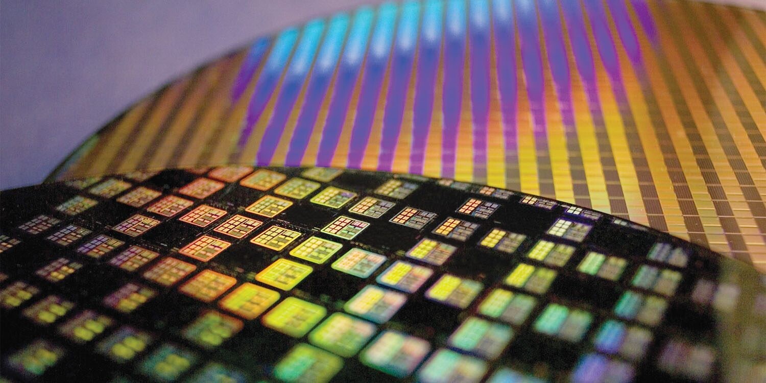
Intel Core i9-10850K Coming to Retail Channel After All, New Celeron Parts Listed

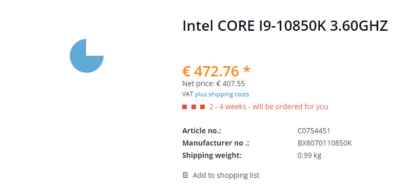
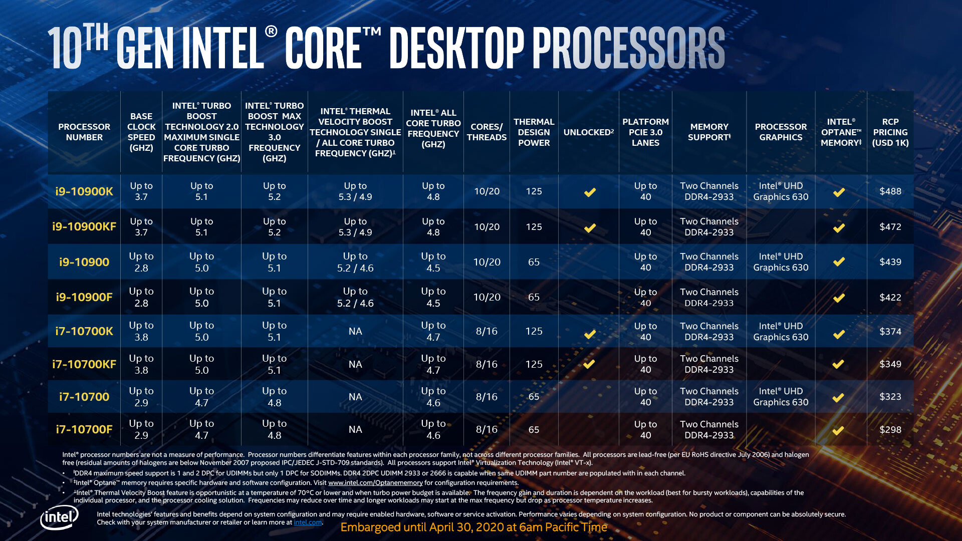
Intel's upcoming Core i9-10850K desktop processor, which was earlier believed to be an OEM-exclusive, is coming to the DIY retail channel after all. The 10-core Socket LGA1200 processor surfaced on retailers Cyclotron and LambdaTek as pre-orders, priced at 472€ and £459, including taxes, which aligns with its rumored USD $449 pre-tax price Stateside. At these prices, the i9-10850K is closer in price to the locked i9-10900 than to the top i9-10900K part.

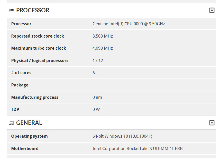
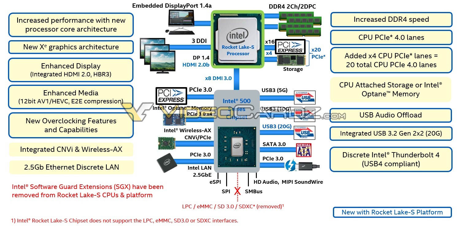
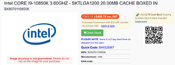
Based on the 14 nm "Comet Lake-S" silicon, the Core i9-10850K is a 10-core/20-thread processor clocked up to 5.20 GHz, with 20 MB of L3 cache. Where it differs from the i9-109xx series is the lack of the Thermal Velocity Boost (TVB) feature. You still get an unlocked multiplier. The i9-10850K is hence provides a roughly $50 saving over the i9-10900K to give up the 100 MHz higher clock speed enabled by TVB. In the retail channel, the chip goes by the SKU "BX8070110850K."

Intel has "Something Big to Share" on September 2nd

Intel just sent out press invites to what is likely an online media event slated for September 2, 2020. The spells nothing other than a one-liner "We have something big to share..." with the September 2 date. Everyone has a theory as to what this could be, depending on who you ask. The Verge has a valid theory pointing to this being a formal launch of the 11th Gen Core "Tiger Lake" mobile processors on the basis of several notebook manufacturers slating their "Tiger Lake" based notebook launches on "Fall 2020."

We believe this could be a desktop-related unveil, possibly a performance preview or teaser of the company's 11th Gen "Rocket Lake-S" processor. Why September? Because September 2020 is going to be a busy month for AMD and NVIDIA, with both launching their next-gen consumer graphics architectures, product lines; and more interestingly, AMD rumored to launch its "Zen 3" microarchitecture in some shape or form. A Ryzen 4000 "Vermeer" product launch could trigger Intel to at least preview "Rocket Lake-S," as it's the first client-desktop microarchitecture in 5 years to introduce IPC gains on the backs of new "Cypress Cove" CPU cores that are a 14 nm back-port of "Willow Cove." It wouldn't surprise us if Intel shed more light on the performance throughput of its big new Xe graphics processors.

Intel Core i7 "Rocket Lake" Chips to be 8-core/12-thread?

It's been rumored for some time now, that the 14 nm "Rocket Lake-S" silicon has no more than 8 CPU cores, giving Intel's product managers some segmentation headaches between the Core i7 and Core i9 brand extensions. The current 10th Gen Core i9 chips are 10-core/20-thread, and Core i7 8-core/16-thread. The 10th Gen Core i5 chips are 6-core/12-thread, and this won't change with the 11th Gen "Rocket Lake." What will change, however, are the core-counts of the Core i7 and Core i9 processors, according to a leaked roadmap slide scored by VideoCardz.

With no more than 8 "Cypress Cove" cores on the "Rocket Lake-S" silicon, the 11th Gen Core i9 will be 8-core/16-thread. The 11th Gen Core i7, however, will be 8-core/12-thread. We don't know how this would work out, but Intel dropped hints toward it with the current 10th Gen Core "Comet Lake," whereby end-users have the ability to toggle HyperThreading (HTT) on a per-core basis. Older generations of Intel processors only allowed a global toggle of HTT. This would mean 4 out of 8 cores on the Core i7 "Rocket Lake-S" will have HTT permanently disabled. We predict that two of these will likely be the processor's favored cores, capable of sustaining the highest boost clocks under the Turbo Boost Max 3.0 algorithm, to which the OS thread scheduler will send the maximum traffic. The roadmap slide also suggests that Intel could standardize the vPro feature-set to its unlocked "K" processors with the 11th Gen.

Bad Intel Quality Assurance Responsible for Apple-Intel Split?

Apple's decision to switch from Intel processors for its Mac computers to its own, based on the Arm architecture, has shaken up the tech world, even though rumors of the transition have been doing rounds for months. Intel's first official response, coupled with facts such as Intel's CPU technology execution being thrown completely off gear due to foundry problems; pointed toward the likelihood of Intel not being able to keep up with Apple's growing performance/Watt demands. It turns out now, that Intel's reasons are a lot more basic, and date back to 2016.

According to a sensational PC Gamer report citing former Intel principal engineer François Piednoël, Apple's dissatisfaction with Intel dates back to some of its first 14 nm chips, based on the "Skylake" microarchitecture. "The quality assurance of Skylake was more than a problem," says Piednoël. It was abnormally bad. We were getting way too much citing for little things inside Skylake. Basically our buddies at Apple became the number one filer of problems in the architecture. And that went really, really bad. When your customer starts finding almost as much bugs as you found yourself, you're not leading into the right place," he adds.

Samsung Provides One-Stop Foundry Design Environment with the Launch of SAFE Cloud Design Platform

Samsung Electronics Co., Ltd., a world leader in advanced semiconductor technology, today announced the launch of 'Samsung Advanced Foundry Ecosystem (SAFE ) Cloud Design Platform (CDP)' for fabless customers, in collaboration with Rescale, a leader in high performance computing (HPC) applications in the cloud. The key highlight feature of Samsung foundry's first SAFE Cloud Design Platform is that it provides a virtual environment to design chips in the cloud. By accessing this platform through the cloud, customers can immediately start designing at anytime and anywhere.

To maximize customers' design convenience, SAFE CDP supports a very secure design condition that has verified with cloud companies. In addition, customers can utilize various Electronic Design Automation (EDA) tools offered by multiple vendors such as Ansys, Cadence, Mentor, a Siemens business and Synopsys. Gaonchips, one of Samsung Foundry's Design Solution Partners, has already tested the SAFE CDP on its 14 nm automotive project using Cadence's Innovus Implementation System and has successfully reduced its design run-time by 30 percent compared to current on-premise execution.

Intel Showcases Intelligent Edge and Energy-efficient Performance Research

This week at the 2020 Symposia on VLSI Technology and Circuits, Intel will present a body of research and technical perspectives on the computing transformation driven by data that is increasingly distributed across the core, edge and endpoints. Chief Technology Officer Mike Mayberry will deliver a plenary keynote, "The Future of Compute: How Data Transformation is Reshaping VLSI," that highlights the importance of transitioning computing from a hardware/program-centric approach to a data/information-centric approach.

"The sheer volume of data flowing across distributed edge, network and cloud infrastructure demands energy-efficient, powerful processing to happen close to where the data is generated, but is often limited by bandwidth, memory and power resources. The research Intel Labs is showcasing at the VLSI Symposia highlights several novel approaches to more efficient computation that show promise for a range of applications - from robotics and augmented reality to machine vision and video analytics. This body of research is focused on addressing barriers to the movement and computation of data, which represent the biggest data challenges of the future," said Vivek K. De, Intel fellow and director of Circuit Technology Research, Intel Labs.

Intel "Willow Cove" Backported to 14nm is "Cypress Cove"?

Intel's 11th generation Core "Rocket Lake-S" desktop processor is fascinating as it introduces Intel's first CPU core IPC uptick in about half a decade. Until now, it was rumored that "Rocket Lake-S" features a back-port of Intel's "Willow Cove" CPU cores to the 14 nm silicon fabrication process. It turns out that Intel doesn't want to call these cores "Willow Cove," which make their debut with the 10 nm+ "Tiger Lake" mobile processors later this Summer. Enter "Cypress Cove." A Moore's Law is Dead video presentation sheds light on this mysterious new codename.

Apparently, "Cypress Cove" is the codename Intel is using to refer to the CPU cores Intel is building with its latest CPU core IP on older 14 nm process. Owing to the process, the IPC of these cores may be different from the "Willow Cove" cores on "Tiger Lake," and to avoid confusion, Intel possibly choosing to give it a different internal codename. In other words, Moore's Law is Dead believes that "Cypress Cove" may not offer the alleged 25% IPC gains over "Skylake" that you could expect instead from "Willow Cove" cores in "Tiger Lake."

Intel "Rocket Lake-S" a Multi-Chip Module of 14nm Core and 10nm Uncore Dies?

VLSI engineer and industry analyst, @chiakokhua, who goes by "Retired Engineer" on Twitter, was among the very first voices that spoke about 3rd gen Ryzen socket AM4 processors being multi-chip modules of core- and uncore dies built on different silicon fabrication processes, which was an unbelievable theory at the time. He now has a fantastic theory of what "Rocket Lake-S" could look like, dating back to November 2019, which is now re-surfacing on tech communities. Apparently, Intel is designing these socket LGA1200 processors to be multi-chip modules, similar to "Matisse" in some ways, but different in others.

Apparently, "Rocket Lake-S" is a multi-chip module of a 14 nm die that holds the CPU cores; and 10 nm die that holds the uncore components. AMD "Matisse" and "Vermeer" too have such a division of labor, but the CPU cores are located on dies with a more advanced silicon fabrication process (7 nm), than the die with the uncore components (12 nm).

Intel 8-core/16-thread "Rocket Lake-S" Processor Engineering Sample 3DMarked

The "Rocket Lake-S" microarchitecture by Intel sees the company back-port its next-generation "Willow Cove" CPU core to the existing 14 nm++ silicon fabrication process in the form of an 8-core die with a Gen12 Xe iGPU. An engineering sample of one such processor made it to the Futuremark database. Clocked at 3.20 GHz with 4.30 GHz boost frequency, the "Rocket Lake-S" ES was put through 3DMark "Fire Strike" and "Time Spy," with its iGPU in play, instead of a discrete graphics card.

In "Fire Strike," the "Rocket Lake-S" ES scores 18898 points in the physics test, 1895 points in the graphics tests, and an overall score of 1746 points. With "Time Spy," the overall score is 605, with a CPU score of 4963 points, and graphics score of 524. The 11th generation Core "Rocket Lake-S" processor is expected to be compatible with existing Intel 400-series chipset motherboards, and feature a PCI-Express gen 4.0 root complex. Several 400-series chipset motherboards have PCIe gen 4.0 preparation for exactly this. The increased IPC from the "Willow Cove" cores is expected to make the 8-core "Rocket Lake-S" a powerful option for gaming and productivity tasks that don't scale across too many cores.

Intel Discontinues 8th Gen Core "Coffee Lake" Desktop Processor Family

Intel today issued a product change notice announcing the discontinuation of its 8th generation Core desktop processor family, and models of Pentium Gold and Celeron processors based on the 14 nm "Coffee Lake" silicon. The PCN covers every 8th gen SKU in the retail- and OEM channels. The company set key dates for the discontinuation. The lineup is discontinued as of June 1, 2020. Suppliers and OEM customers can last order their products on December 18, 2020. The last product shipment is slated for June 4, 2021. It's likely that the 9th generation Core desktop processor family will be follow next year. The 8th generation Core "Coffee Lake" saw the first increase in core counts for Intel's mainstream desktop processor family in close to a decade.

Qualcomm FastConnect 6900/6700 Bring 6 GHz Wi-Fi 6E & Bluetooth 5.2 To New Mobile Devices

Qualcomm Technologies Inc, launches a flagship portfolio of mobile connectivity systems that represent the most advanced Wi-Fi 6E offerings of their kind. Building upon our leading Wi-Fi 6 and Bluetooth audio technology features, the Qualcomm FastConnect 6900 and Qualcomm FastConnect 6700 mobile connectivity systems feature the fastest available Wi-Fi speeds in the industry (up to 3.6 Gbps) on a mobile Wi-Fi offering, VR-class low latency and Bluetooth advancements delivering immersive audio experiences for classic and emerging LE Audio use cases.

"With the introduction of the FastConnect 6900 and 6700 solutions, Qualcomm Technologies is redefining the mobile experience by extending the power of Wi-Fi 6 into the 6 GHz band and advancing wireless audio with cutting-edge integrated Bluetooth 5.2 features," said Dino Bekis, vice president and general manager, mobile and compute connectivity, Qualcomm Technologies, Inc. "These innovations enable us to further break away from the pack and deliver a connectivity portfolio optimized to accelerate global adoption across multiple smartphone tiers."

Intel Rocket Lake CPU Appears with 6 Cores and 12 Threads

We have been hearing a lot about Intel's Rocket Lake lineup of processors. They are supposed to be a backport of Willow Cove 10 nm core, adapted to work on a 14 nm process for better yielding. Meant to launch sometime around late 2020 or the beginning of 2021, Rocket Lake is designed to work on the now existing LGA1200 socket motherboards, which were launched just a few days ago along with Intel Comet Lake CPUs. Rocket Lake is there to supply the desktop segment and satisfy user demand, in light of lacking 10 nm offers for desktop users. The 10 nm node is going to present only on mobile/laptop and server solutions before it comes to the desktop.

In the latest report on 3D Mark, the hardware leaker TUM APISAK has found a Rocket Lake CPU running the benchmark and we get to see first specifications of the Rocket Lake-S platform. The benchmark ran on 6 core model with 12 threads, that had a base clock of 3,5 GHz. The CPU managed to boost up to 4,09 GHz, however, we are sure that these are not final clocks and the actual product should have even higher frequencies. Paired with Gen12 Xe graphics, the Rocket Lake platform could offer a very nice alternative to AMD offerings if the backport of Willow Cove goes well. Even though it is still using a 14 nm node, performance would be good. The only things that would be sacrificed (from backporting) are die space and efficiency/heat.
Intel Rocket Lake Benchmark Report

SMIC Begins Mass-Production of 14nm FinFET SoCs for Huawei HiSilicon

Semiconductor Manufacturing International Corporation (SMIC), the state-backed Mainland Chinese semiconductor foundry, announced that it commenced mass-production of 14 nm FinFET SoCs for Huawei's HiSilicon subsidiary, a mere one month since Huawei shifting chip orders from TSMC to it. The company is manufacturing Kirin 710A is a revision of the original Kirin 710 SoC from 2018, built on SMIC's 14 nm node. The 4G-era SoC is capable of powering mid-range smartphones for Huawei's Honor brand, and uses an Arm big.LITTLE setup of Cortex A53 and Cortex A57 cores. This represents a major milestone not just for SMIC, but also Huawei, which has seen the company's isolation from cutting-edge overseas fabs such as TSMC. Much of Huawei's fate is riding on the success of SMIC's next-generation N+1 node, which purportedly offers a 57 percent energy-efficiency gain over 14 nm FinFET, rivaling sub-10 nm nodes such as 7 nm; enabling Huawei to build 5G-era SoCs.

Gigabyte Says Intel Z490 Chipset Motherboards Will Support 11th Gen "Rocket Lake-S"

Maybe it's hard to fathom an Intel chipset that actually supports more than a single generation of CPU designs; and if so, you're forgiven, because it seems the blue giant has mostly forgotten of thinking about platform longevity and upgradeability. However, we might be in for a rare treat, if the words from a Gigabyte representative are to be taken seriously. In a Q&A regarding Gigabyte's latest generation Z490 motherboards, a user questioned the Gigabyte representatives whether their Z490-based platforms would support upcoming Rocket Lake designs. The answer, which came with a caveat of "I don't know if this should be made public", was that yes: Z490 will support Rocket Lake-S.

If true, this may shed some light on why motherboard manufacturers have given so much importance to PCIe 4.0 marketing on their Z490 motherboards... Whose chipset doesn't support PCIe 4.0 from the get-go. However, with next-generation Rocket Lake-S expectedly sporting the same 14 nm fabrication process albeit with a new microarchitecture, a wider DMI 3.0 8x band, Intel's high-performance Xe graphics architecture design and PCIe 4.0 support on a platform level, it does begin to make sense that manufacturers would mention PCIe 4.0 support on the current Z490. Because if CPU compatibility is maintained, that means that users looking to drop-in a Rocket Lake-S CPU will at the very least be able to enjoy 20 lanes of PCIe 4.0 in these ready-made motherboards.

Intel 10th Generation Comet Lake Desktop Processors and 400-Series Chipsets Announced, Here's what's New

Intel today launched its 10th generation Core desktop processor family and its companion Intel 400-series chipsets. Based on the 14 nm++ silicon fabrication process and built in the new LGA1200 package, the processors are based on the "Comet Lake" microarchitecture. The core design of "Comet Lake" and its IPC are identical to those of "Skylake," however Intel brought significant enhancements to the processor's clock-speed boosting algorithm, increased core- or thread counts across the board, and introduced new features that could interest enthusiasts and overclockers. The uncore component remains largely unchanged from the previous-generation, with support for DDR4 memory and PCI-Express gen 3.0. Use of these processors requires a new socket LGA1200 motherboard, they won't work on older LGA1151 motherboards. You can install any LGA115x-compatible cooler on LGA1200, provided it meets the thermal requirements of the processor you're using.

At the heart of the 10th generation Core processor family is a new 10-core monolithic processor die, which retains the same basic structure as the previous-generation 8-core "Coffee Lake Refresh" die, and 4-core "Skylake." The cores are arranged in two rows, sandwiched by the processor's uncore and iGPU blocks. A ring-bus interconnect binds the various components. The cache hierarchy is unchanged from previous generations as well, with 32 KB each of L1I and L1D caches; 256 KB of dedicated L2 cache per core, and 20 MB of shared L3 cache. The iGPU is the same Gen 9.5 based UHD 630 graphics. As we mentioned earlier, much of Intel's innovation for the 10th generation is with the processor's microcode (boosting algorithms).
Intel Core i9-10900K 10th Gen Intel Core Desktop Comet Lake Lineup 10th Gen Intel Core Desktop Comet Lake Lineup 10th Gen Intel Core Desktop Comet Lake Lineup

AMD Updates Ryzen 3 1200 CPU with Zen+ Architecture

AMD has reportedly updated its Ryzen 3 1200 CPU with Zen+ architecture and is now offering it to consumers. Featuring a configuration of 4 cores with 4 threads, this CPU can operate anywhere from 3.1 GHz (base) to 3.4 GHz in boost frequency. Having originally launched in July of 2017, just under three years ago, AMD decided to refresh this CPU with Zen+ architecture, which brought improvements like a tiny IPC increase, better turbo boost speeds, faster caches and better memory controller for better support of faster DDR4 modules.

The new "Zen+" revision has the same specifications as the older model, however, the only difference is the newer 12 nm manufacturing process and some of the architecture changes of Zen+. The rest of the specifications like clock speeds are the same. The CPU is listed by a German supplier for €54.73 or about $60. This revision carries a different part number, under the code "YD1200BBM4KAFBOX", where the older 14 nm model was "YD1200BBM4KAEBOX".
AMD Ryzen 3 1200 12nm Zen+ Edition

Huawei Moves 14 nm Silicon Orders from TSMC to SMIC

Huawei's subsidiary, HiSilicon, which designs the processors used in Huawei's smartphones and telecommunications equipment, has reportedly moved its silicon orders from Taiwan Semiconductor Manufacturing Company (TSMC) to Semiconductor Manufacturing International Corporation (SMIC), according to DigiTimes. Why Huawei decided to do is move all of the 14 nm orders from Taiwanese foundry to China's largest silicon manufacturing fab, is to give itself peace of mind if the plan of the US Government goes through to stop TSMC from supplying Huawei. At least for the mid-tier chips built using 14 nm node, Huawei would gain some peace as a Chinese fab is a safer choice given the current political situation.

When it comes to the high-end SoCs built on 7 nm, and 5 nm in the future, it is is still uncertain how will Huawei behave in this situation, meaning that if US cuts off TSMC's supply to Huawei, they will be forced to use SMIC's 7 nm-class N+1 node instead of anything from TSMC. Another option would be Samsung, but it is a question will Huawei put itself in risk to be dependant on another foreign company. The lack of 14 nm orders from Huawei will not be reflecting much on TSMC, because whenever someone decides to cut orders, another company takes up the manufacturing capactiy. For example, when Huawei cut its 5 nm orders, Apple absorbed by ordering more capacity. When Huawei also cut 7 nm orders, AMD and other big customers decided to order more, making the situation feel like there is a real fight for TSMC's capacity.
Silicon Wafer

Intel Comet Lake Pricing Leaked

Listings for Intel's Comet Lake-S desktop processors have been found on DirectDial a Canadian PC retailer. Comet Lake-S is the next generation of chips using Intel's 14 nm process and will feature up to 10 cores and 20 threads. The leaked prices reveals a significant fall in per core pricing from Coffee Lake chips however Ryzen 3000 will continue to dominate in pricing if this leak is correct, especially considering the lack of including cooling with the new Intel chips. Below are the leaked prices with direct conversions to USD.
  • Core i9-10900 (10 cores / 20 threads, 2.8 GHz to 5.2 GHz): $679 CAD = $486 USD
  • Core i7-10700K (8 cores / 16 threads, 3.8 GHz to 5.1 GHz): $585 CAD = $419 USD
  • Core i7-10700 (8 cores / 16 threads, 2.9 GHz to 4.8 GHz): $506 CAD = $362 USD

Intel Planning 14nm "Ozark Lake" 16-core Processor for Spring 2021

TechPowerUp has learned that Intel is planning to bring 16 cores onto the mainstream desktop platform by Spring 2021 by implementing a similar chip-design philosophy as AMD: MCMs. The new "Ozark Lake" processor will pack up to 16 cores and 32 threads by decoupling the "core" and "uncore" components of a typical Intel mainstream processor.

Intel will leverage the additional fiberglass substrate floor-space yielded from the new LGA1700 package to create a multi-chip module that has two [kinds of] dies, the "core complex" and the "uncore complex." The core complex is a 14 nm die purely composed of CPU cores and an EMIB interconnect. There will be as many as 16 "Skylake" cores in a conventional ringbus layout, and conventional cache hierarchy (256 KB L2$ and up to 2 MB/core L3$). The lack of uncore components and exclusive clock and voltage domains will allow the CPU cores to attain Thermal Velocity Boost Pro speeds of up to 6.00 GHz, if not more.

Intel Core i9-10980HK Detailed: 8-core Mobile Monstrosity that Boosts up to 5.30 GHz

In no mood to cede mobile performance leadership to AMD and its Ryzen 9 4900HS processor, Intel is readying its new flagship mobile part, the Core i9-10980HK. Based on the 14 nm "Comet Lake-H" silicon, this chip packs an 8-core/16-thread CPU with a maximum boost speed (aka "Thermal Velocity Boost") of 5.30 GHz, while maintaining an aggressive power target of 45 W TDP. This should put the chip's performance somewhere between the desktop Core i7-9700K and the Core i9-9900K, both of which have TDP rated at 95 W, although the chip could perform very close to the latter at gaming, thanks to its 300 MHz higher boost frequency. Intel is expected to launch the 10th generation Core i9 H-series processors on April 2nd, around the same time when NVIDIA launches its mobile GeForce RTX 20 Super series.

Samsung Announces Industry's First EUV DRAM with Shipment of First Million Modules

Samsung Electronics Co., Ltd., the world leader in advanced memory technology, today announced that it has successfully shipped one million of the industry's first 10 nm-class (D1x) DDR4 (Double Date Rate 4) DRAM modules based on extreme ultraviolet (EUV) technology. The new EUV-based DRAM modules have completed global customer evaluations, and will open the door to more cutting-edge EUV process nodes for use in premium PC, mobile, enterprise server and datacenter applications.

"With the production of our new EUV-based DRAM, we are demonstrating our full commitment toward providing revolutionary DRAM solutions in support of our global IT customers," said Jung-bae Lee, executive vice president of DRAM Product & Technology at Samsung Electronics. "This major advancement underscores how we will continue contributing to global IT innovation through timely development of leading-edge process technologies and next-generation memory products for the premium memory market."
Samsung EUV DDR4

Intel Rocket Lake-S Platform Detailed, Features PCIe 4.0 and Xe Graphics

Intel's upcoming Rocket Lake-S desktop platform is expected to arrive sometime later this year, however, we didn't have any concrete details on what will it bring. Thanks to the exclusive information obtained by VideoCardz'es sources at Intel, there are some more details regarding the RKL-S platform. To start, the RKL-S platform is based on a 500-series chipset. This is an iteration of the upcoming 400-series chipset, and it features many platform improvements. The 500-series chipset based motherboards will supposedly have an LGA 1200 socket, which is an improvement in pin count compared to LGA 1151 socket found on 300 series chipset.

The main improvement is the CPU core itself, which is supposedly a 14 nm adaptation of Tiger Lake-U based on Willow Cove core. This design is representing a backport of IP to an older manufacturing node, which results in bigger die space due to larger node used. When it comes to the platform improvements, it will support the long-awaited PCIe 4.0 connection already present on competing platforms from AMD. It will enable much faster SSD speeds as there are already PCIe 4.0 NVMe devices that run at 7 GB/s speeds. With RKL-S, there will be 20 PCIe 4.0 lanes present, where four would go to the NVMe SSD and 16 would go to the PCIe slots from GPUs. Another interesting feature of the RKL-S is the addition of Xe graphics found on the CPU die, meant as iGPU. Supposedly based on Gen12 graphics, it will bring support for HDMI 2.0b and DisplayPort 1.4a connectors.
Intel Rocket Lake-S Platform

AMD Radeon RX 590 GME is a Dressed Up RX 580: No more 12nm, Lower Performance

When AMD pushed out the Radeon RX 590 in late-2018, its key spec was that the "Polaris 20" die had been ported to GlobalFoundries 12LPP (12 nm) silicon fabrication node, yielding headroom to dial up clock speeds over the 14 nm RX 580. The underlying silicon was labeled "Polaris 30" as it was the second major version of the "Polaris 10" die. NVIDIA's GeForce GTX 16-series beat the RX 590 both in performance and price, with even the GTX 1650 Super performing on-par, and the GTX 1660 beating it. It turns out that AMD has a lot of unsold 14 nm "Polaris 20" inventory to go around, and it wants to release them out as the new RX 590 GME.

An Expreview review of an XFX-branded RX 590 GME confirms that the the chip is indeed based on the "Polaris 20 XTR" silicon which is built on the 14 nm process. The card has GPU clock speeds that appear similar to reference clock speeds of the RX 590, with 1460 MHz base compared to 1469 MHz of the original RX 590. But this is where the similarities end. In its testing, Expreview found that the RX 590 GME is on average 5% slower than the RX 590, and performs halfway between the RX 580 and the original RX 590, which are differentiated by a roughly 10% performance gap. The 5% performance deficit would put the RX 590 GME on par with the new RX 5500 XT 4 GB, and trading blows with the GTX 1650 Super. Thankfully, the RX 590 GME is priced lower than RX 590 cards (about 7.7% cheaper), and could be very region-specific. The fact that the RX 590 GME is being sold with full AIB partner branding and retail packaging, shows that this isn't an OEM-only product. Read the complete review in the source link below.
RX 590 GME Front View RX 590 GME PCB RX 590 GME Polaris 20 GPU RX 590 GME GPU-Z RX 590 GME Performance

Intel Restarts 14 nm Operations in Costa Rica, Aims to Increase Capacity for Xeon Output

Intel has decided to restart operations in its previously winded-down Costa Rica facilities. An Intel Product Change Notification (PCN) for their Cascade Lake Xeon Scalable processors shows that the company has added Costa Rica to its three other "Test and Finish" sites - the other three are located in Penang (Malaysia), Kulim (Malaysia) and Vietnam. Intel's aim is to guarantee a "continuous supply" of the affected processors - namely, Cascade Lake second-generation Xeon Scalable processors in the Silver, Gold and Platinum lines (in both boxed and tray SKUs).

This move, which will be done in phases. The first implementation of the Costa Rica operations will be effective on April 19th, with the remaining operations to come online on August 3rd. Intel expects to reduce dependency on their other three Test and Finish sites, while being able to bolster final production capacity by some 25% with this move.

NVIDIA GeForce MX350 and MX330 Surface, Pascal Based Entry mGPUs

NVIDIA's GeForce MX-series mobile GPU line exists so notebook manufacturers can put the NVIDIA logo on their products and boast of gaming capabilities. The company is giving finishing touches to its new GeForce MX330 and MX350 chips, based on the "Pascal" architecture. The MX330 is the company's second rebrand of the MX150 that's based on the 14 nm "GP108" silicon. It's equipped with 384 CUDA cores, and up to 2 GB of GDDR5 memory across a 64-bit wide memory interface. NVIDIA increased the clock speeds to 1531 MHz base, and 1594 MHz GPU Boost (compared to 1227/1468 MHz of the MX150), while remaining in the 25 W TDP envelope.

The MX350, on the other hand, is based on the 14 nm "GP107" silicon, is equipped with 640 CUDA cores, and 2 GB of GDDR5 memory across the same 64-bit bus width as the MX330; but has aggressive power-management that lends it a TDP of just 20 W, despite 66% more CUDA cores than the MX330. Both chips are easily capable of handling non-gaming tasks on typical 1080p / 1440p notebooks; but can game only at 720p thru 1080p, with low-to-mid settings.
Return to Keyword Browsing
Apr 23rd, 2024 14:21 EDT change timezone

New Forum Posts

Popular Reviews

Controversial News Posts