News Posts matching #14 nm

Return to Keyword Browsing

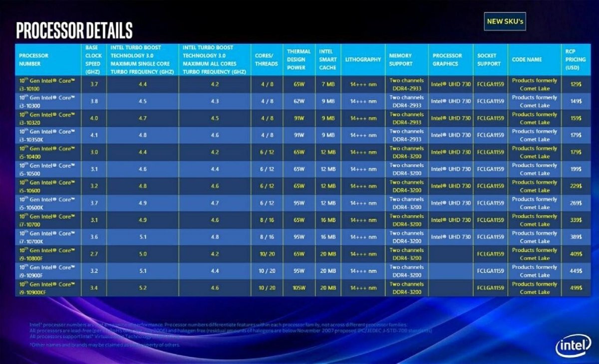
Intel Core i3-10100 Put Through SANDRA, Beats i3-9100 by 31% in Multimedia Tests

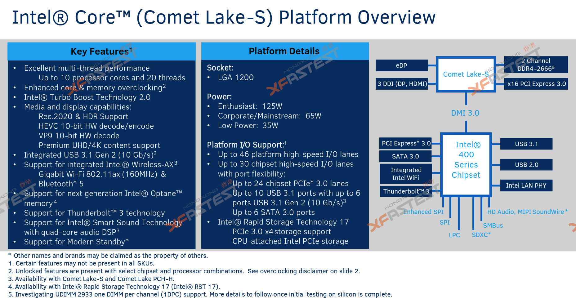
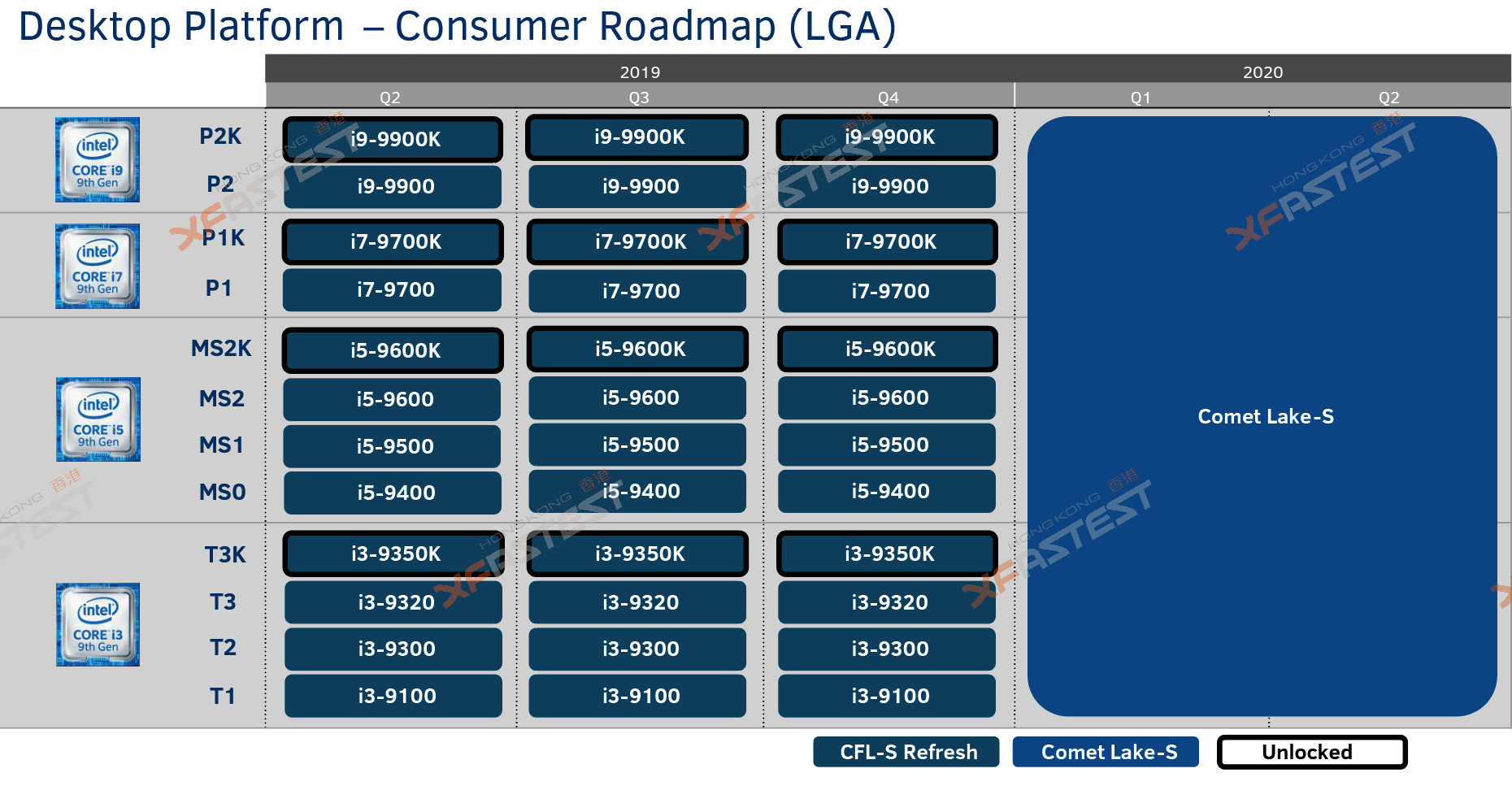
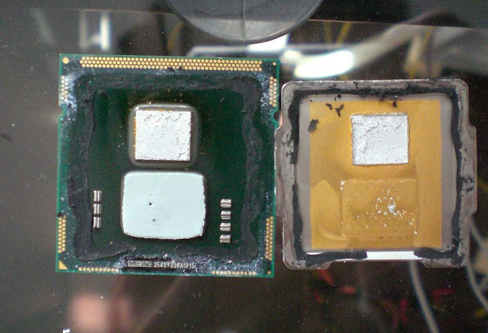
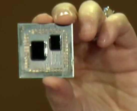
Intel's 10th generation Core desktop processor lineup, based on the 14 nm "Comet Lake" silicon, will begin with the Core i3-10100 succeeding the Core i3-9100 and i3-8100. To squeeze the most out of the microarchitecture that's essentially identical to "Skylake," Intel has decided to enable HyperThreading across the Core processor family, which means the i3-10100 is a 4-core/8-thread chip. Interestingly, Intel has given it just 6 MB of shared L3 cache. It's likely that the slightly beefed up i3-103xx will be differentiated with 8 MB of L3 cache. The chip has the same 3.60 GHz nominal frequency, and an unknown degree of Turbo Boost. The current-gen i3-9100 features Turbo Boost, so it's likely that its successor will also get the feature.

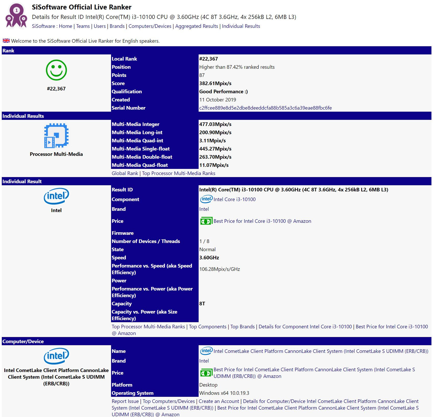
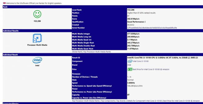
A SiSoft SANDRA online database entry for the i3-10100 surfaced, where it has an overall score of 382.61 MPix/s using multimedia tests, a significal step up from the roughly 290 MPix/s of the i3-9100 (a 31 percent performance increase). This increase in performance can be attributed to HyperThreading, as SANDRA's multimedia tests leverage it efficiently. Intel is expected to launch the Core i3-10100 around the $120 mark, competing with AMD's Ryzen 3 3200G.

Next-Gen Intel Core i3 to Sport Hyper Threading?

TUM_APISAK has done of his well-regarded snoopings again, and this one could have relevant information for the democratization of threads in next-gen Intel products. Intel has been slowly (as they can) increasing the amount of cores and threads in their respective product lines across i3, i5, and i7 CPUs after AMD's Ryzen onslaught. Luckily, from two core, four-thread Core i3 of a few years ago, we now seem to be entering a new era for entry-level computing, with a new SiSoftware benchmark seemingly showing an Intel next-gen "Comet Lake" Core i3 CPU sporting 4 physical threads with Hyper Threading enabled (so, basically, the equivalent of Skylake Core i7's from just three years ago).

The benchmark submission lists what appears to be a four-core, eight-thread Core i3-10100. It sports a 3.6 GHz base clock, which likely isn't final, so take that frequency with a grain of salt. This shuffle in the low-end definitely means an upscale in Intel's more powerful lineups, with HyperThreading likely being active for all of their product stack across Comet Lake - 4C, 8T Core i3; 6C, 12T Core i5; 8C, 16T Core i7; and a likely 10C, 20T Core i9 10900K that straddles the line between consumer and HEDT platforms. Of course, remember these are still built upon the 14 nm process, give or take a few "+" symbols, so don't expect too much in terms of energy efficiency gains.

Intel Discontinues Almost the Entire 7th Generation Core Desktop Processor Series

Intel late Thursday, through a product change notification, announced the discontinuation of almost its entire 7th generation Core "Kaby Lake" desktop processor series. This includes most chips across the Core i3, Core i5, Core i7, Pentium, and Celeron desktop chips based on the 14 nm+ "Kaby Lake-S" silicon, across both retail boxed and tray packages. These chips formed Intel's main product lineup through 2017, and had to be quickly succeeded by the 8th generation "Coffee Lake" with the advent of AMD Ryzen. To clear out its inventory, Intel will accept discontinuance orders for these chips until April 2020. A discontinuance order can only be placed by a customer who has previously ordered these exact chips. The last of these orders will be shipped out by October 2020.

Intel Marketing Tries to Link Stability to Turbo Boost

There is no correlation between CPU frequency boosting behavior and system stability. Intel today launched its "10th generation" Core X HEDT processors, with core-counts ranging between 10 to 18, priced between $590 and $978. Based on the 14 nm "Cascade Lake-X" silicon, these chips have the same exact IPC as "Skylake" circa 2015, but offer nearly double the number of cores to the Dollar compared to the 9th generation Core X series; and add a couple of useful instruction sets such as DLBoost, which accelerates DNN training/building; a few more AVX-512 instructions, and an updated Turbo Boost Max 3.0 algorithm. The chips offer clock-speed bumps over the previous generation.

Intel's main trade-call for these processors? Taking another stab at AMD for falling short on boost frequency in the hands of consumers. "The chip that hits frequency benchmarks as promised, our new #CoreX -series processor, provides a stable, high-performance platform for visual creators everywhere," reads the Intel tweet, as if to suggest that reaching the "promised" clock speed results in stability. AMD was confronted with alarming statistics of consumers whose 3rd generation Ryzen processors wouldn't reach their advertised boost frequencies. The company released an updated AGESA microcode that fixed this.

Intel 10th Gen Core X "Cascade Lake-X" Pricing and Specs Detailed

Ahead of their October 7th product launch and November availability, we have confirmation of the specifications and pricing of Intel's 10th generation Core X "Cascade Lake-X" HEDT processors in the LGA2066 package. These chips feature compatibility with existing socket LGA2066 motherboards with a UEFI BIOS update, although several motherboard manufacturers are launching new products with some of the latest connectivity options, such as 2.5 GbE wired Ethernet, and 802.11ax Wi-Fi 6 WLAN.

The 10th generation Core X HEDT processor family is based on the new 14 nm++ "Cascade Lake" silicon, which comes with hardware fixes against several classes side-channel vulnerabilities, and introduces an updated instruction-set that includes more AVX-512 instructions, and the new DLBoost instruction. DLBoost leverages new fixed-function hardware on silicon to accelerate AI deep-learning neural-set building and training by up to 5 times. Intel's first wave of 10th gen Core X lineup is rather slim, with just four processor models. The company did away with the Core i7 brand extension, as core-counts in the mainstream desktop segment have already reached 8-core. The lineup now begins at 10-core/20-thread, with the chip's full 48-lane PCI-Express and 4-channel DDR4 interfaces enabled across the board. All models feature the "XE" brand extension, and feature unlocked base-clock multipliers.

Intel's 14nm Chip Shortage Continues

Intel is constantly having troubles with its silicon manufacturing business lately. Firstly the late delivery of 10 nm, then the shortage of 14 nm chips that started all the way back in 2018. Despite the making of $1 Billion investment into extending its 14 nm production capacity, there seems to be no end of troubles in sight.

According to sources close to DigiTimes, 14 nm production has fallen short of demand again and will likely cause many notebook manufacturers to delay their products to 2020. Most likely victim of this delay is the newly announced 10th generation mobile CPUs codenamed Comet Lake. Those CPUs were supposed to be built using Intel's "14nm++" revision of 14 nm technology which targets higher CPU frequencies and improved efficiency, but most likely due to continued shortage of 14nm, there will be only a few notebooks powered by these chips. As the source suggests, many manufacturers are likely to delay the launch of their products to 2020, when this situation is supposed to be resolved.

Intel Cascade Lake-X Core i9-10980XE Put Through Its Paces in GeekBench

Intel's upcoming Extreme Edition Core i9-10980XE from the Cascade Lake-X family. Cascade Lake-X (CSL-X) will be Intel's next take on the High End Desktop (HEDT) systems. The Core i9-10980XE is pegged as the flagship on that lineup, sporting an 18-core, 36-thread design, and are still based on Intel's 14 nm process node. These processors will be pin-compatible with Intel's LGA 2066 platform. Caches are expected to be set at 1.125 MB, 18 MB and 24.75 MB of L1, L2 and L3.

Base clocks set in the Geekbench 4 entry are set at 4.1 GHz, with a maximum boost of 4.7 GHz. That's a lot of frequency on a 14 nm CPU with 18 cores; if previous entries on the Intel HEDT family (such as the i9-9980XE) sported a 165 W TDP with clocks of 3.0 GHz and 4.4 GHz respectively, it seems highly unlikely that Intel will keep the same TDP for the i9-10980XE - and even if they do, power consumption will certainly be higher. Those reported clocks for the i9-10980XE may not be right, however - we don't know the conditions of the test run.

Dozens of GIGABYTE Intel 400-series Chipset Motherboards Show Up at the EEC

Intel is inching closer to the launch of its socket LGA1200 mainstream desktop platform based on its 400-series chipset and 14 nm "Comet Lake-S" silicon. The platform provides a forward upgrade path to the company's 10 nm "Ice Lake-S" processors when they come out. "Comet Lake-S" is a derivative of the "Skylake" microarchitecture that's been scaled up to 10 CPU cores, and HyperThreading enabled across the board, with clock speeds pushed to the limits of the 14 nm silicon fabrication process. The TDP of some of these parts is reportedly set as high as 125 W. GIGABYTE is ready with dozens of motherboards for these processors, based on one of five chipsets - Z490, H470, Q470, B460, and H410.

The Intel Z490 Express will be the top-end chipset geared toward gamers and enthusiasts wanting to overclock their processors. The H470 will be a slight step down, and possibly lack multi-GPU and CPU overclocking support. The Q470 is its twin with certain enterprise-relevant features. The B460 is the mid-range chipset, targeting a spectrum of users including gamers who don't overclock their CPU. The H410 will be the entry-level chipset for everyone else. What's interesting about GIGABYTE's list of motherboards filed for regulatory clearance from the Eurasian Economic Commission, is that is looks partial. There are far too few AORUS-branded products.

Alleged Leaked Details on Intel Comet Lake-S Platform Require... You Guessed It... A New Platform

Intel's development of their Core architecture in the post-Ryzen world has been slow, with solutions slowly creeping up in core counts with every new CPU release - but much slowly than rival AMD's efforts. Before Intel can capitalize on a new, more scalable and power-efficient architecture, though, it has to deliver performance and core count increases across its product line to stay as relevant as possible against a much revitalized rival. Enter Comet Lake-S: the desktop parts of Intel's new round of consumer CPUs, which will reportedly see an increase in the maximum core count to a 10-core design. This 10-core design, however, comes with an increase in power consumption (up to 135 W), and the need, once again, for beefier power delivery systems in a new, LGA 1200 package (with 9 more pins that the current LGA 1151).

The move to a new socket and the more stringent power requirements give Intel the opportunity to refresh its chipset offerings once again. If everything stays the same (and there's no reason it should change), new Z470 and Z490 chipsets should be some of the higher tier offerings for builders to pair with their motherboards. The new Comet Lake-S CPUs will still be built in the now extremely refined 14 nm process, and allegedly keep the same 16 PCIe 3.0 lanes as current Coffee Lake Refresh offerings. The new CPU offerings from Intel are expected to roll out in Q1 2020.

Intel's CEO Blames 10 nm Delay on being "Too Aggressive"

During Fortune's Brainstorm Tech conference in Aspen, Colorado, Intel's CEO Bob Swan took stage and talked about the company, about where Intel is now and where they are headed in the future and how the company plans to evolve. Particular focus was put on how Intel became "data centric" from "PC centric," and the struggles it encountered.

However, when asked about the demise of Moore's Law, Swan detailed the aggressiveness that they approached the challenge with. Instead of the regular two times improvement in transistor density every two years, Swan said that Intel has always targeted better and greater densities so that it would stay the leader in the business.

Intel "Comet Lake" Not Before 2020, "Ice Lake-S" Not Before Q3-2020, Roadmap Suggests

Earlier this week, news of Intel's 10th generation Core "Comet Lake" processors did rounds as the company's short-term response to AMD's 3rd generation Ryzen processors. According to slides leaked to the web by Hong Kong-based tech publication XFastest, "Comet Lake" isn't Intel's short-term reaction to "Zen 2," but rather all it has left to launch. These processors won't launch before 2020, the slide suggests, meaning that AMD will enjoy a free rein over the processor market until the turn of the year, including the all-important Holday shopping season.

More importantly, the slide suggests that "Comet Lake" will have a market presence spanning Q1 and Q2 2020, meaning that the 10 nm "Ice Lake" won't arrive on the desktop platform until at least Q3 2020. It's likely that the LGA1200 platform which debuts with "Comet Lake" will extend to "Ice Lake," so consumers aren't forced to buy a new motherboard within a span of six months. The platform diagram put out in another slide junks the idea of an on-package MCM of the processor and PCH dies (which was likely ripped off from the "Ice Lake-Y" MCM platform diagram).

Intel 10th Generation Core "Comet Lake" Lineup Detailed

Intel's short-term reaction to AMD's 3rd generation Ryzen processor family is the 10th generation Core "Comet Lake." These processors are based on existing "Skylake" cores, but have core-counts increased at the top-end, and HyperThreading enabled across the entire lineup. The Core i3 series are now 4-core/8-thread; the Core i5 series a 6-core/12-thread, the Core i7 series are 8-core/16-thread, and the new Core i9 series are 10-core/20-thread. Besides core-counts, Intel has given its 14 nanometer node one last step of refinement to come up with the new 14 nm+++ nodelet. This enables Intel to significantly dial up clock speeds across the board. These processors come in the new LGA1159 package, and are not backwards-compatible with LGA1151 motherboards. These chips also appear to feature an on-package PCH, instead of chipset on the motherboard.

Leading the pack is the Core i9-10900KF, a 10-core/20-thread chip clocked at 4.60 GHz with 5.20 GHz Turbo Boost, 20 MB of shared L3 cache, native support for DDR4-3200, and a TDP of 105 W. Intel's new 10-core die appears to physically lack an iGPU, since none of the other Core i9 10-core models offer integrated graphics. For this reason, all three processor models have the "F" brand extension denoting lack of integrated graphics. The i9-10900KF is closely followed by the i9-10900F clocked at 4.40/5.20 GHz, the lack of an unlocked multiplier, and 95 W TDP rating. The most affordable 10-core part is the i9-10800F, clocked at 4.20 GHz with 5.00 GHz boost, and a TDP of just 65 W. Intel has set ambitious prices for these chips. The i9-10900KF is priced at $499, followed by the i9-10900F at $449, and the i9-10800F at $409.

NVIDIA Manufacturing Turing GPUs at Samsung Korea Fab, 11nm?

During our disassembly of the GeForce RTX 2060 Super, we noticed a shocking detail. The 12 nm "TU106" GPU on which it is based, has the marking "Korea." We know for a fact that TSMC does not have any fabs there. The only Korean semiconductor manufacturer capable of contract-manufacturing a piece of silicon as complex as a GPU, for a designer with the energy-efficiency OCD as NVIDIA, is Samsung.

What makes this interesting is that Samsung does not officially have a 12 nm FinFET process. It has 14 nm, and the 11LPP, a 11 nm nodelet, which the company designed to compete with TSMC 12 nm. It would hence be really interesting to hear from NVIDIA on whether they've scaled out the "TU106" to 14LPP, or down to 11LPP at Samsung. It's interesting to note that the shrink in transistor sizes in these nodelets doesn't affect die-sizes. We hence see no die-size difference between these Korea-marked chips, and those marked "Taiwan." We've reached out to NVIDIA for comment.

Update July 3rd: NVIDIA got back to us
NVIDIAThe answer is really simple and these markings are not new. Other Turing GPUs have had these markings in the past. The chip is made at TSMC, but packaged in various locations. This one was done in Korea, hence why his says "Korea".

On an unrelated note: We already use both TSMC and Samsung, and qualify each of them for every process node. We can't comment in any further detail on future plans, but both remain terrific partners.

AMD Confirms Ryzen 3000 "Matisse" Features Soldered IHS

AMD senior technical marketing manager Robert Hallock, responding to a specific question on Twitter, confirmed that the 3rd generation Ryzen processors do feature soldered integrated heatspreaders (IHS). Soldering as an interface material is preferred as it offers better heat transfer between the processor die and the IHS, as opposed to using a fluid TIM such as pastes. "Matisse" will be one of the rare few examples of a multi-chip module with a soldered IHS. The package has two kinds of dies, one or two 7 nm "Zen 2" 8-core CPU chiplets, and one 14 nm I/O Controller die.

The most similar example of such a processor would be Intel's "Clarkdale" (pictured below), which has its CPU cores sitting on a 32 nm die, while the I/O, including memory controller and iGPU, are on a separate 45 nm die. On-package QPI connects the two. Interestingly, Intel used two different sub-IHS interface materials for "Clarkdale." While the CPU die was soldered, a fluid TIM was used for the I/O controller die. It would hence be very interesting to see if AMD solders both kinds of dies under the "Matisse" IHS, or just the CPU chiplets. Going by Hallock's strong affirmative "Like a boss," we lean toward the possibility of all dies being soldered.
Image Credit: TheLAWNOOB (OCN Forums)

Intel Pushes the Panic Button with Core i9-9900KS

With 7 nm AMD Ryzen 3000 processor family expected to make landfall early-July, and "Ice Lake" nowhere in sight, a panicked Intel announced the development of the Core i9-9900KS 8-core/16-thread LGA1151 processor. Based on the 14 nm "Coffee Lake Refresh" silicon, this processor has a base-frequency of 4.00 GHz, up from 3.60 GHz of the original; and an all-core Turbo Boost frequency of 5.00 GHz, identical to the original i9-9900K, which has its max-turbo set at 5.00 GHZ, too. A revamped Turbo Boost algorithm is expected to yield significant gains in multi-core performance. The company didn't reveal TDP, pricing, or availability.

AMD Ryzen 9 3000 is a 16-core Socket AM4 Beast

AMD is giving finishing touches to its 3rd generation Ryzen socket AM4 processor family which is slated for a Computex 2019 unveiling, followed by a possible E3 market availability. Based on the "Matisse" multi-chip module that combines up to two 8-core "Zen 2" chiplets with a 14 nm I/O controller die, these processors see a 50-100 percent increase in core-counts over the current generation. The Ryzen 5 series now includes 8-core/16-thread parts, the Ryzen 7 series chips are 12-core/24-thread, while the newly created Ryzen 9 series (designed to rival Intel Core i9 LGA115x), will include 16-core/32-thread chips.

Thai PC enthusiast TUM_APISAK confirmed the existence of the Ryzen 9 series having landed himself with an engineering sample of the 16-core/32-thread chip that ticks at 3.30 GHz with 4.30 GHz Precision Boost frequency. The infamous Adored TV leaks that drew the skeleton of AMD's 3rd generation Ryzen roadmap, referenced two desktop Ryzen 9 parts, the Ryzen 9 3800X and Ryzen 9 3850X. The 3800X is supposed to be clocked at 3.90 GHz with 4.70 GHz boost, with a TDP rating of 125W, while the 3850X tops the charts at 4.30 GHz base and a staggering 5.10 GHz boost. The rated TDP has shot up to 135W. We can now imagine why some motherboard vendors are selective with BIOS updates on some of their lower-end boards. AMD is probably maximizing the clock-speed headroom of these chips out of the box, to preempt Intel's "Comet Lake" 10-core/20-thread processor.

Intel Drivers Reveal 400, 495 Series Chipsets for Comet Lake, Ice Lake - New Year, New Socket, Same 14 nm Process

Data extracted from Intel's latest Server Chipset Driver (10.1.18010.8141) mentions support for new chipsets, which will bring about compatibility for the company's upcoming Comet Lake chips. Comet Lake, if you remember, is Intel's latest gasp in the 14 nm process for CPUs, and should bring up to 10 cores to the consumer segment. The increase in maximum number of cores will naturally be Intel's justification for the need for new chipsets and sockets, due to "electrical incompatibilities" and increased requirements in the power delivery subsystem.

If you're looking for the latest and greatest changes to Intel's architecture and manufacturing process, you'll have to wait for Ice Lake, for which the 495 series chipset brings compatibility. But for that one, you'll have to wait until 2020. Let's see what AMD's Ryzen 2 brings to the table against Intel's current (and up to 10 nm Comet Lake) offerings. Even excluding platform longevity, AMD's architecture and core density really has been giving Intel a run for its money.

Intel 10nm Ice Lake to Quantitatively Debut Within 2019

Intel put out interesting details about its upcoming 10 nanometer "Ice Lake" CPU microarchitecture rollout in its recent quarterly financial results call. The company has started qualification of its 10 nm "Ice Lake" processors. This involves sending engineering samples to OEMs, system integrators and other relevant industry partners, and getting the chips approved for their future product designs. The first implementation of "Ice Lake" will not be a desktop processor, but rather a low-power mobile SoC designed for ultraportables, codenamed "Ice Lake-U." This SoC packs a 4-core/8-thread CPU based on the "Sunny Cove" core design, and Gen11 GT2 integrated graphics with 64 execution units and nearly 1 TFLOP/s compute power. This SoC will also support WiFi 6 and LPDDR4X memory.

Intel CEO Bob Swan also remarked that the company has doubled its 10 nm yield expectations. "On the [10 nm] process technology front, our teams executed well in Q1 and our velocity is increasing," he said, adding "We remain on track to have volume client systems on shelves for the holiday selling season. And over the past four months, the organization drove a nearly 2X improvement in the rate at which 10nm products move through our factories." Intel is prioritizing enterprise over desktop, as "Ice Lake-U" will be followed by "Ice Lake-SP" Xeon rollout in 2020. There was no mention of desktop implementations such as "Ice Lake-S." Intel is rumored to be preparing a stopgap microarchitecture for the desktop platform to compete with AMD "Matisse" Zen 2 AM4 processors, codenamed "Comet Lake." This is essentially a Skylake 10-core die fabbed on existing 14 nm++ node. AMD in its CES keynote announced an achievement of per-core performance parity with Intel, so it could be interesting to see how Intel hopes 10 "Skylake" cores match up to 12-16 "Zen 2" cores.

Tesla Dumps NVIDIA, Designs and Deploys its Own Self-driving AI Chip

Tesla Motors announced the development of its own self-driving car AI processor that runs the company's Autopilot feature across its product line. The company was relying on NVIDIA's DGX processors for Autopilot. Called the Tesla FSD Chip (full self-driving), the processor has been deployed on the latest batches of Model S and Model X since March 2019, and the company looks to expand it to its popular Model 3. Tesla FSD Chip is an FPGA of 250 million gates across 6 billion transistors crammed into a 260 mm² die built on the 14 nm FinFET process at a Samsung Electronics fab in Texas. The chip packs 32 MB of SRAM cache, a 96x96 mul/add array, and a cumulative performance metric per die of 72 TOPS at its rated clock-speed of 2.00 GHz.

A typical Autopilot logic board uses two of these chips. Tesla claims that the chip offers "21 times" the performance of the NVIDIA chip it's replacing. Elon Musk referred to the FSD Chip as "the best chip in the world," and not just on the basis of its huge performance uplift over the previous solution. "Any part of this could fail, and the car will keep driving. The probability of this computer failing is substantially lower than someone losing consciousness - at least an order of magnitude," he added.
Slides with on-die details follow.

Intel Unleashes 56-core Xeon "Cascade Lake" Processor to Preempt 64-core EPYC

Intel late Tuesday made a boat-load of enterprise-relevant product announcements, including the all important update to its Xeon Scalable enterprise processor product-stack, with the addition of the new 56-core Xeon Scalable "Cascade Lake" processor. This chip is believed to be Intel's first response to the upcoming AMD 7 nm EPYC "Rome" processor with 64 cores and a monolithic memory interface. The 56-core "Cascade Lake" is a multi-chip module (MCM) of two 28-core dies, each with a 6-channel DDR4 memory interface, totaling 12-channel for the package. Each of the two 28-core dies are built on the existing 14 nm++ silicon fabrication process, and the IPC of each of the 56 cores are largely unchanged since "Skylake." Intel however, has added several HPC and AI-relevant instruction-sets.

To begin with, Intel introduced DL Boost, which could be a fixed-function hardware matrix multiplier that accelerates building and training of AI deep-learning neural networks. Next up, are hardware mitigation against several speculative execution CPU security vulnerabilities that haunted the computing world since early-2018, including certain variants of "Spectre" and "Meltdown." A hardware fix presents lesser performance impact compared to a software fix in the form of a firmware patch. Intel has added support for Optane Persistent Memory, which is the company's grand vision for what succeeds volatile primary memory such as DRAM. Currently slower than DRAM but faster than SSDs, Optane Persistent Memory is non-volatile, and its contents can be made to survive power-outages. This allows sysadmins to power-down entire servers to scale down with workloads, without worrying about long wait times to restore uptime when waking up those servers. Among the CPU instruction-sets added include AVX-512 and AES-NI.

AMD Ryzen 3000 "Zen 2" BIOS Analysis Reveals New Options for Overclocking & Tweaking

AMD will launch its 3rd generation Ryzen 3000 Socket AM4 desktop processors in 2019, with a product unveiling expected mid-year, likely on the sidelines of Computex 2019. AMD is keeping its promise of making these chips backwards compatible with existing Socket AM4 motherboards. To that effect, motherboard vendors such as ASUS and MSI began rolling out BIOS updates with AGESA-Combo 0.0.7.x microcode, which adds initial support for the platform to run and validate engineering samples of the upcoming "Zen 2" chips.

At CES 2019, AMD unveiled more technical details and a prototype of a 3rd generation Ryzen socket AM4 processor. The company confirmed that it will implement a multi-chip module (MCM) design even for their mainstream-desktop processor, in which it will use one or two 7 nm "Zen 2" CPU core chiplets, which talk to a 14 nm I/O controller die over Infinity Fabric. The two biggest components of the IO die are the PCI-Express root complex, and the all-important dual-channel DDR4 memory controller. We bring you never before reported details of this memory controller.

Intel Core i9-9900F Makes an Appearance in SiSoft Sandra: No iGPU, No Unlocked Multiplier

Intel has been playing with the release of multiple of their 14 nm ++ processors without any integrated graphics tech, such as the Intel Core i5-9400F, or the iGPU-less, unlocked Core i9-9900KF. However, as strange as it may seem, a quick look online still shows the i9-9900KF selling for more ($582.50) than its complete i9-9900 sibling.

The Core i9-9900F, as caught in SiSoft's Sandra, is likely simply a locked-down version of Intel's Core i9-9900, since delidding of Intel's Core i5-9400F has shown that the silicon real-estate for the iGPU is still there - as such, this likely isn't an effort from Intel to reduce the silicon used for graphics and pass on the savings to customers. At the most, this is Intel launching products that may carry defective iGPUs from the production process and still be able to sell them - though Intel does seem to be looking not to budge on its profit margin, even on these "crippled" CPUs.

China-based SMIC to Start Manufacture of 14 nm-class Chips in 2H 2019

As R&D costs for new, smaller manufacturing nodes grow at unprecedented rates across the industry, a new player is set to enter the 14 nm process manufacture competition: China-based SMIC (Semiconductor Manufacturing International Corporation). The company is looking to throw its hat on the lucrative 14 nm process, filling its offerings portfolio under the 28 nm it currently offers as its denser process.

The company expects its 95% yield rate to offer its customers a trusted platform that might help it increase revenue for further investment on its 10 nm and 7 nm EUV nodes, which the company is pursuing (despite other industry veterans, such as former AMD-manufacturing arm GLOBALFOUNDRIES having ceased development on). Manufacturing technology that's competitive with the western world's, and that's developed in-country, is paramount for China's intention of reducing its dependence of foreign technology, which is why this is such a big step for the company and the company's aspirations.

Intel's FinFET-Based Embedded MRAM is Ready for Production

A report via EETimes slates Intel's own working MRAM (Magnetoresistive Random-Access Memory) is ready for production in high-volume manufacturing. MRAM is a nonvolatile memory technology, meaning that it retains information even if there is a change in powerstate (ie, power loss), meaning that it's more akin to a storage device than to, say, RAM.

But why does MRAM matter, really? Well, MRAM is being developed as a long-term candidate to a universal memory solution, replacing both DRAM (a volatile memory technology) and NAND flash (a nonvolatile one), since node scaling with these technologies is becoming increasingly harder. MRAM promises better-scaling (at the foundry level) processes, with much higher yield rates. The fact that MRAM has been demonstrated to be able to achieve 1 ns settling times, better than the currently accepted theoretical limits for DRAM, and much higher write speeds (as much as thousands of times faster) compared to NAND flash.

Intel Rolls Out the 4 GHz Pentium Gold G5620 Processor

Intel rolled out its first Pentium-branded processor with 4.00 GHz clock-speed, the Pentium Gold G5620 (retail SKU: BX80684G5620). The chip replaces the G5600 on top of the entry-level product stack. Based on the 14 nm "Coffee Lake" microarchitecture, it packs a 2-core/4-thread CPU clocked at 4.00 GHz without Turbo Boost. 256 KB of L2 cache per core and 4 MB of shared L3 cache are also offered. The integrated graphics solution is Intel's workhorse UHD Graphics 630, with 24 execution units. The dual-channel DDR4 integrated memory controller supports up to 64 GB of DDR4-2400 memory. The chip's TDP is rated at 65W. Pricing is up in the air, with retail channel shortages expected to swing the chip on both sides of the $100-mark. Availability is slated for early-March, 2019.
Return to Keyword Browsing
Apr 19th, 2024 04:56 EDT change timezone

New Forum Posts

Popular Reviews

Controversial News Posts