News Posts matching #32 nm

Return to Keyword Browsing

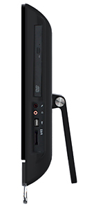
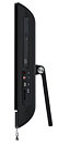
GIGABYTE introduces the GB-AEBN All-In-One PC

GIGABYTE introduces a fully modulated AIO PC model to answer any requirements in the most time and cost efficient way. Whether you want a turnkey, a highly customized or only a barebone product, the GB-AEBN solution can answer your needs, as the entire system is broken down into integrated and standardized modules that can be easily and quickly upgraded or replaced. With this modulated concept, the specifications of the GB-AEBN can be calibrated towards the needs of any kind of end user, and therefore it can be suitable for your targets.

Thanks to its modulated concept, we are able to adapt most of the GB-AEBN parts to deliver any kind of end-user advantage, and you can easily modify them afterwards. The GB-AEBN solution supports components from any supplier complying to our product's form factors (Intel's AIO Mini-ITX standard, slim ODD bay, 3.5'' SATA bay, etc.).

Intel Readies 32 nm Cedar View Atom Processors for Late 2011

Intel will give its category-defining Atom processor its next big update in Q4, 2011. Codenamed "Cedar Trail", Intel's next Atom processor will use the latest manufacturing process technologies, and up the feature-set a bit. The Cedar Trail platform combines the Atom "Cedar View" processor with a chipset similar to Intel NM10 from the current "Pine Trail". The platform is laid out in a similar 2-chip package. The first chip embeds a dual-core x86-64 processor, an integrated memory controller that supports single-channel DDR3 memory, and a new DirectX 10.1 compliant integrated GPU that supports 1080p video playback, it connects to the chipset over DMI.

Cedar View Atom processor will be built on Intel's 32 nm process. The new process chops TDP by 30%, while allowing higher clock speeds. Some of the first Cedar View processors are dual-core. Designed for low-power desktops and nettops, the Atom D2500 runs at 1.86 GHz, has no HyperThreading Technology (HTT), has 1 MB of shared cache, and 10W TDP. In contrast, the 45 nm "Pine View" Atom D525 processor achieves 1.83 GHz at 13W TDP. Intel will have a higher-performing part, the Atom D2700. The D2700 is clocked at 2.13 GHz, features HTT, and the TDP remains at 10W.

Sandy Bridge-Based Pentium Dual-Core G840 Processor Surfaces

The first Intel Pentium branded processor based on the Sandy Bridge architecture surfaced in China. The Pentium Dual-Core G840 as it's identified, is said to be based on the 32 nm dual-core silicon. It differs from Core i3 dual-core processors in having no HyperThreading technology (one thread per core), and 3 MB of L3 cache enabled. The AVX instruction set also seems to be lacking according to the CPU-Z screenshot.

The Pentium G840 is clocked at 2.80 GHz, with a base clock of 100 MHz, and 28x multiplier. The embedded Intel HD Graphics GPU is clocked at 850 MHz, with 1100 MHz GPU Turbo Boost frequency. The processor cores lack Turbo Boost. The chip has a TDP of 65W. Pricing and availability details are awaited, though expect this LGA1155 chip to cost under $100.

AMD 'Bulldozer' CPUs Slated for June

AMD is said to have finalized the shipping dates of its new high-end processor lineup. The company's new nameless lineup of high-end desktop processors will be released to market in the second half of June. The new processors will be built on the 32 nm manufacturing process, and will be based on the much talked about Bulldozer architecture. The reason it's "nameless" is because there's no processor brand (such as Athlon or Phenom) attached to it. The lineup will consist of AMD FX8000 series octo-core processors, AMD FX6000 series hexa-core processors, and AMD FX4000 series quad-core processors. The chip will feature high-speed DDR3 integrated memory controllers, but will lack integrated graphics. AMD will release as many as eight processor models. To support the processors, AMD's partners in the motherboard industry will release socket AM3+ motherboards based on AMD 9-series chipsets, around the same time.

Intel Gives Core i3 and Core i5 Dual-Core Processors K0 Stepping Update

Intel is giving some existing 32 nm "Clarkdale" based Core i3 and Core i5 processors an update. The processors will transition to the new K0 stepping from the existing C2 stepping. The parts that will be made on the K0 silicon are Core i3 models 530 (new sSPEC: SLBX7), 540 (new sSPEC: SLBTD) and Core i5 models 650 (new sSPEC: SLBTJ), 660/661 (SLBTK/SLBTB), 670 (SLBTL). Newer and upcoming models such as the i3-550, i3-560, i5-665K, and i5-680 are already being built on the K0 stepping die. Motherboards will require a BIOS update to support the new K0 stepping processors.

The K0 stepping change includes the following highlights:
  • New S-spec and MM numbers for the converting products
  • Extended CPUID will change from 0x00020652 to 0x00020655
  • Host RevID will change from 0x12 to 0x18
  • K0 stepping package is pin compatible with C2 stepping package
  • Adds Processor Context ID (PCID) support
The revised older SKUs that are built on K0 stepping will be market-available by October 16.

Intel Reveals New Logos and a Die Shot of Second Generation Core Processors

At the keynote of Intel Developer Forum 2010, the silicon giant gave a sneak-peak into its upcoming processor brand, revealing new product logos (case badges), and a die-shot of the Sandy Bridge quad-core silicon. Intel retains the Core i3, Core i5, and Core i7 brand identifiers, but refers to the family of processors based on the Sandy Bridge architecture as second-generation Core processors or the 2011 Intel Core processors. For the same reason, processor model numbers start with the 2000 series as detailed in this article.

The die shot reveals integration of the IGP-embedded northbridge component completely into the processor die. In "Clarkdale" Core i3 and Core i5 processors, the northbridge component was present on a separate die from the CPU die, with a QPI link connecting the two dies on the same package. The Sandy Bridge quad-core die is known to feature 6 MB of L3 cache, a dual-channel DDR3 IMC, and a DirectX 10.1 compliant graphics processor. Apart from merely driving graphics, the IGP also feature several media-acceleration features that speed up video encoding. Sandy Bridge is fabricated on the 32 nanometer HKMG process. The evolution of Intel's architectures is shown on the last picture. The "Nehalem" chip there is the Lynnfield quad-core processor that completely lacks an IGP, "Westmere" is the Clarkdale dual-core processor that has an IGP and memory controller on a second (larger) 45 nm die. The chip to the right is a 32 nm Sandy Bridge that integrates a quad-core chip with an IGP-embedded northbridge.

Bulldozer-based Orochi and Fusion Llano Die Shots Surface in GlobalFoundaries Event

The first official die-shots of the first Bulldozer architecture derivative, the eight-core "Orochi" Opteron die was displayed at Global Technology Conference, by GlobalFoundries, AMD's principal foundry-partner. While AMD did not give out a die-map to go with it, the structures we can make out are four Bulldozer modules holding two cores and a shared L2 cache each, a L3 cache spread across four blocks that's shared between all cores, the northbridge-portion cutting across the die at the center, and the integrated memory controller along its far-right side. Various I/O portions are located along the other three sides.

Next up is the Llano die. This is AMD's very first Fusion APU (accelerated processing unit) die. It is based on the K10 architecture and integrates a graphics processor and northbridge completely into one die. It precedes APUs based on the Bobcat architecture. Fortunately, there is a die-map at hand, which shows four K10 cores with dedicated 1 MB L2 caches per core, no L3 cache, an integrated SIMD array that holds 480 stream processors. The GPU component is DirectX 11 compliant. Other components include an integrated northbridge, integrated memory controller, integrated PCI-Express root complex, and HyperTransport interface to the chipset.

AMD Details Bulldozer Processor Architecture

AMD is finally going to embrace a truly next generation x86 processor architecture that is built from ground up. AMD's current architecture, the K10(.5) "Stars" is an evolution of the more market-successful K8 architecture, but it didn't face the kind of market success as it was overshadowed by competing Intel architectures. AMD codenamed its latest design "Bulldozer", and it features an x86 core design that is radically different from anything we've seen from either processor giants. With this design, AMD thinks it can outdo both HyperThreading and Multi-Core approaches to parallelism, in one shot, as well as "bulldoze" through serial workloads with a broad 8 integer pipeline per core, (compared to 3 on K10, and 4 on Westmere). Two almost-individual blocks of integer processing units share a common floating point unit with two 128-bit FMACs.

AMD is also working on a multi-threading technology of its own to rival Intel's HyperThreading, that exploits Bulldozer's branched integer processing backed by shared floating point design, which AMD believes to be so efficient, that each SMT worker thread can be deemed a core in its own merit, and further be backed by competing threads per "core". AMD is working on another micro-architecture codenamed "Bobcat", which is a downscale implementation of Bulldozer, with which it will take on low-power and high performance per Watt segments that extend from all-in-One PCs all the way down to hand-held devices and 8-inch tablets. We will explore the Bulldozer architecture in some detail.

Toshiba Introduces Double Data Rate Toggle Mode NAND In MLC And SLC Configurations

Toshiba America Electronic Components, Inc ., (TAEC) is introducing 32 nm double data rate Toggle Mode NAND, in multi-level cell (MLC) versions with densities of 64 Gb, 128 Gb and 256 Gb and single-level cell (SLC) versions with densities of 32 Gb, 64 Gb and 128 Gb. Toggle Mode NAND features a faster interface than conventional or "legacy" asynchronous NAND memory with lower power consumption than competing synchronous DDR NAND product offerings.

Toshiba DDR Toggle Mode 1.0 NAND has a fast interface rated at 133 megatransfers per second (MT/s), compared to 40 MT/s for legacy SLC single data rate NAND, which makes it suitable for high performance solid state storage applications including enterprise storage. Since it uses an asynchronous interface similar to that used in conventional NAND, the Toshiba DDR Toggle Mode NAND requires no clock signal, which means that it uses less power and has a simpler system design compared to competing synchronous NAND alternatives. The DDR interface in Toggle Mode NAND uses a Bidirectional DQS to generate input/output signals (I/Os) using the rising and falling edge of the write erase signal. Toggle Mode NAND also has on-die termination to help achieve less crosstalk.

Intel Core i7 970 Starts Surfacing at e-Tailers

Intel's next six-core desktop processor, the Core i7 970, has started to surface on online stores, with UK-based Digital Fusion listing it for an uncomfortable £ 600.44 excluding applicable tax. The listing confirms the processor's clock speed to be 3.20 GHz, while it is known to be based on the 32 nm Gulftown die. The processor comes in the LGA1366 package, and should be compatible with all LGA1366 motherboards, with some requiring BIOS updates.

Intel to Release Core i7 990X Extreme Edition Six-Core Processor in Q4 2010

Intel is working on a newer high-end processor SKU based on its 32 nm "Gulftown" six-core design, the Core i7 990X Extreme Edition. It is reportedly slated for Q4 2010. As with most other Extreme Edition SKUs, the 990X will feature a higher default BClk multipler, and a higher resulting clock speed. Like the Core i7 980X Extreme Edition, it will feature an unlocked BClk multipler to help with overclocking. Gulftown features six cores on a monolithic die, with a triple-channel DDR3 IMC, and 12 MB of L3 cache. The launch of 990X is said to have been pulled forward by a quarter, as it was earlier reported to launch in Q1 2011.

The other six-core processor that is said to release before the 990X is the Core i7 970, a standard (non-XE, limited BClk multiplier) SKU that will be positioned in the upper-Performance segment, above current Core i7 quad-core SKUs. The Core i7 970 is slated for Q3 2010.

AMD Demonstrates Graphics Processing Power of Llano Fusion APUs

AMD demonstrated its first Fusion APU (accelerated processing unit), which is a "fusion" between a processor and a graphics processor. The first such processor in the works is based on the 32 nm silicon fabrication technology, codenamed Llano, and fuses a quad-core processor with a DirectX 11 compliant GPU. AMD's Rick Bergman showed off a wafer of the Llano APUs, but it didn't stop there. Rick surprised the press when he went on to claim that the APU can power Aliens vs. Predator in DirectX 11 mode, with a reasonable level of detail, which was demonstrated. Find a video of the same at the source.

Intel Intros Core i5 680 and Pentium E5500

Intel introduced two new dual-core processors, the high-end Core i5 680, and the value-segment Pentium Dual-Core E5500. The former is an LGA1156 chip that runs on Intel P55, H55, H57, Q55, Q57 chipsets, while the latter is an LGA775 chip that works on most recent LGA775 motherboards. The Core i5 680 uses the 32 nm based Clarkdale core. At 3.60 GHz (27 x 133 MHz) with a Turbo Boost speed of 3.86 GHz, the i5 680 is expected to be the fastest dual-core processor ever made. Its embedded Intel HD Graphics controller is clocked at 733 MHz. It has L2 caches of 256 KB per core, and a shared L3 cache of 4 MB. It supports two channels of DDR3 memory. With HyperThreading enabled, the chip gives the OS four logical CPUs to deal with. It has a TDP of 73W.

The Pentium Dual-Core E5500 is based on the 45 nm Wolfdale-2M core, it has a clock speed of 2.80 GHz (14 x 200 MHz), and FSB speed of 800 MHz. It has a shared L2 cache of 2 MB, and TDP of 65W. While the Core i5 680 is priced at US $294, the E5500 goes for $75. All prices are per-piece in 1000 unit tray quantities.

Intel to Introduce 8-core Xeon Nehalem-EX, 6-core Westmere-EP Processors This Month

Intel is set to introduce a series of eight-core Xeon server processors later this month, that are capable of running in four-socket servers. With HyperThreading technology enabled, each core can handle two threads, taking the logical CPU count on such servers up to 64. Each Nehalem-EX chip has 8 CPU cores with dedicated L2 caches of 256 KB, a shared L3 cache of 24 MB, and Turbo Boost technology that helps conserve power while also stepping up performance when needed. The die also features a memory controller with four DDR3 memory channels. Being based on the Nehalem architecture, the chips are built on the 45 nm HKMG process.

In related news, Intel will also introduce Westmere-EP processors later this month. These chips will be based on the 32 nm Westmere architecture, and are likely to have 6 cores, up to 12 logical CPUs per chip, 12 MB of L3 cache and three DDR3 memory channels. These chips will be suited for two-socket servers and workstations.

EVGA Names and Details its Dual-LGA1366 Enthusiast Motherboard

EVGA today named its dual-LGA1366 enthusiast-grade motherboard, so far known by the codename W555. After a short contest on the company's forums, the company came up with "EVGA Classified SR-2" for its name. SR stands for "super record" and 2 denoting the dual-socket design. The Classified SR-2 is a an entusiast-grade (read: overclocker friendly) implementation of the Tylersburg platform, supporting Intel socket LGA1366 processors with two QPI links (2P Xeon, etc.) As an addition, the board allows you to do something that's difficult on typical 2P server motherboards: it allows you to mix different models of Xeon processors, provided they're based on the same architecture, and series. For example, you can mix a Xeon 5520 with Xeon 5540. You can also mix a quad-core processor with a six-core processor, provided the quad-core part is based on the Westmere architecture (32 nm), not Nehalem (45 nm).

The board will also let you run a single 2P-capable processor in either sockets. DDR3 memory modules can be non-ECC or even ECC. 2P Xeon DRAM Multipliers / Uncore Multipliers are locked so you will only be able to use maximum 2:8 or 2:10 depending on segment of CPU. EVGA tells that the board supports 4-way SLI on its GTX 285 Classified VGA, but adds that a "future flagship GPU" also supports it. Could this be GeForce GTX 400 series having it as a standard feature? We have to wait and see. 4-way CrossFireX is supported.

AMD to Sample 32 nm Processors Within H1 2010

AMD, in its presentation at the International Solid State Circuits Conference (ISSCC) 2010, presented its plan to build its much talked about 'Fusion' processor platform, codenamed Llano, central to which, is the Accelerated Processing Unit (APU). AMD's APU is expected to be the first design to embed a multi-core x86 CPU and a GPU onto a single die. This design goes a notch ahead of Intel's recently released 'Clarkdale' processor, where Intel strapped a 32 nm dual-core CPU die and a 45 nm northbridge die with integrated graphics, onto an MCM (multi chip module) package. Llano is also expected to feature four processing cores, along with other design innovations.

Some of the most notable announcements in AMD's presentation is that the company will begin sampling the chip to its industry partners within the first half of 2010. The Llano die will be build on a 32 nm High-K Metal Gate process. On this process, each x86 core will be as small as 9.69 mm². Other important components on the Llano die are a DDR3 memory controller, on-die northbridge, and a DirectX 11 compliant graphics core derived from the Evergreen family of GPUs. The x86 cores are expected to run at speeds of over 3 GHz. Each core has 1 MB of dedicated L2 cache, taking the total chip cache size to 4 MB.

Intel Unveils Core i5 6xx, 6x1 Series Dual-Core Processors

Intel today gave a go ahead for the media to publish reviews of its brand new dual-core processors under the Core i5 6xx and Core i5 6x1 series. The processors are based on the new "Clarkdale" processor die, and make use of the company's 32 nm next generation HKMG manufacturing process. Unlike conventional processor packages based on the Nehalem/Westmere architecture, the new processors move the northbridge component of the system onto the processor package, only that it is based on a separate 45 nm die within the package. The 32 nm processor die houses two processor cores along with up to 4 MB of L3 cache, while it is wired to a larger iGPU die which houses the dual-channel DDR3 memory controller, a graphics core, PCI-Express root complex, along with other components traditionally found on northbridge chips.

The first three models in the new Core i5 series are the 3.20 GHz Core i5 650, 3.33 GHz Core i5 660 and 661 (latter has a faster iGPU), and 3.46 GHz Core i5 670. These processors have the LGA-1156 package and are compatible with existing P55 Express chipset (albeit without the iGPU feature), along with the company's new H55 Express and H57 Express chipsets that support the Flexible Display Interface that provides connectivity to the processors' iGPUs. The new processors feature HyperThreading Technology, with which it provides the operating system with four logical CPUs (threads) to deal with, TurboBoost technology which powers down a core and overclocks the other when the task load is low. Pricing and availability will surface when the processors are formally announced, a little later this month. Meanwhile, motherboard manufacturers are ready with boatloads of new motherboard models based on Intel's two new chipsets. A compilation of links to major reviews on the internet can be found in the day's reviews list on the homepage.

ASUS X58 Motherboards First to Support Upcoming 32 nm CPUs

ASUS announced that it is ready to support the upcoming 32nm processor based on the LGA1366 socket and the Intel X58 chipset. This next-generation 32nm infrastructure, supporting six multi-cores, will deliver maximum performance to ASUS X58-based motherboards via a comprehensive BIOS upgrade. Chie-Wei Lin, General Manager of ASUS Motherboard Business said, "This new processor architecture accommodates up to six cores and significantly improves CPU performance. By enabling the architecture in our award-winning X58-based motherboards, we can deliver one of the fastest personal computing platforms in history and we are very excited about it."

ASUS' entire range of X58-based motherboards is ready for the new 32nm processor. For maximum CPU performance and advanced graphics processing enabled by the six cores, users simply need to update the BIOS of their existing X58-based motherboards.

Intel to Release 17 Processors This January 2010

After giving its socket LGA-1156 quad-core processors a flying start, Intel is poised to release not just a couple of more processors in Q1-2010, but as many as 17 new models on January 7 alone, reports suggest. Among these are chips based on the company's new 32 nm manufacturing technology, which gives the manufacturer headroom to up features and performance, while maintaining low thermal and energy footprints.

This is when the company completes its triad of new generation Core family processors, with the Core i3 series of entry-level thru lower-mainstream processors. This triad starts with Core i3 as an entry-point for "smart performance", with Core i5 in the middle delivering "smart performance with Turbo Boost Technology", and Core i7 at the top, delivering "the ultimate in smart performance".

Intel Readies 13 Westmere-based 32 nm Xeon Processors

Outgrowing the known lineup of 32 nm client processors (under the Core family), Intel's upcoming lineup of processors based on the 32 nm Westmere architecture will comprise of no less than 13 models under the Xeon E5000, L5000, X5000, and W3600 series. Among these, there are six hexa-core Xeon processors, including X5680 (3.33 GHz), X5670 (2.93 GHz), X5660 (2.80 GHz), and X5650 (2.66 GHz). X5680 has a TDP of 130W, with the latter three sub 3 GHz models having TDP as low as 95W. There is an energy-efficient L5640 hexa-core model clocked at 2.26 GHz, with TDP at 60W, and a single-socket W3680, clocked at 3.33 GHz with 130W TDP. All these models have six cores, and 12 MB of L3 cache.

Next up, are Intel's first 32 nm quad-core processors: Xeon X5677 (3.46 GHz, 130W), X5647 (3.06 GHz, 95W), E5640 (2.66 GHz, 80W), X5630 (2.53 GHz, 80W), X5620 (2.40 GHz, 80W), and energy efficient L5630 (2.13 GHz, 40W), and L5609 (1.86 GHz, 40W). Except L5609, all these quad-core chips have HyperThreading Technology and Turbo Boost available. The L2 cache amounts for each of these chips is unknown as of now, but should be up to 8 MB, or as low as 4 MB for some models. Most of these chips are slated for release on March 16, 2010.

Dual Core Intel Core i3, Core i5 Processors Start Getting Listed

Over a month ahead of its launch, the first wave of Intel's 32 nm based Core i3 and Core i5 series dual-core processors have been listed on German online store HPM-Computer. The pricing and specifications disclosed by these listing confirm the information that surfaced as early as in July, this year. The series starts with Core i3 500 series processors whose clock speeds range between 2.93 to 3.06 GHz, and continue with Core i5 600 series dual-core processors ranged between 3.20 GHz and 3.43 GHz. While both series feature HyperThreading Technology to give the operating system four logical processors (threads) to work with, the Core i3 processors lack the Turbo Boost feature which the Core i5 chips have.

According to the new listing in which the chips are priced in Euros, the 2.93 GHz Core i3 530 processor is priced at 103.90 EUR, and 3.06 GHz Core i3 540 at 120.90 EUR. The Core i5 600 series lineup includes the 3.20 GHz Core i5 650 priced at 160.90 EUR, 3.33 GHz Core i5 660 and 661 priced at 175.90 EUR, and lead by the 3.43 GHz Core i5 670 priced at a premium 252.90 EUR point. All prices include a 19% applicable tax. The IGP clock speed (750 MHz vs. 900 MHz), differentiates Core i5 660 from 661. It is likely that the price of one of those seems to have entered incorrectly. With these processors, Intel may also introduce the Intel H57 Express chipset, and motherboards by various vendors will soon follow. These processors, however, have the same LGA-1156 socket the "Lynnfield" quad-core processors have, which are currently in the market. They may run on existing P55 Express based motherboards too, according to a recent report.

AMD to Sample Bulldozer Architecture in 2010, Sets Product Priorities

As part of its Financial Analyst Day for 2009, AMD listed out its priorities for the year ahead, looking into 2010. While the company has lived up to its development targets for this year by releasing a full-fledged lineup of PC and server processors built on the 45 nm process, increasing its market share with graphics products, and releasing the first DirectX 11 compliant (back then referred to as 'next generation') GPU, the year ahead looks equally ambitious for AMD.

AMD set the following product priorities for 2010: to deliver four new winning PC platforms in the first half of 2010, improve battery life of its notebook platform, expand homegrown DirectCompute 11 and OpenCL developer tools, propagate DirectX 11 graphics to notebooks, launch the company's first 12-core Opteron processor, and more interestingly, sample the company's next-generation "Bulldozer" architecture to industry customers, along with sampling the company's first Fusion-design "Bobcat" processor, which integrates the CPU with GPU, along with sampling some of the company's first processors built on the 32 nm manufacturing process.

Core i5 650 ''Clarkdale'' Reaches 4.70 GHz on Air-Cooling

Intel's socket LGA-1156 quad-core processors are closely trailed by the company's first processors based on the 32 nm manufacturing process: Core i5 and Core i3 "Clarkdale" dual-core processors. Engineering samples of these processors were evaluated as early as Q2 2009, but one of the first attempts to show the processors' overclocking potential using air-cooling was made very recently. Even prior to that, a low-voltage overclocking feat by Coolaler showed how engineering samples didn't particularly struggle reaching clock speeds close to 4.00 GHz with vCore as low as 0.832V. Romanian tech community Lab501. Lab501 community leader "Monstru" tested the overclocking headroom of a Core i5 650 LGA-1156 dual-core processor (engineering sample) with air-cooling.

The test-bed included a Gigabyte P55 motherboard, the Core i5 650 processor was cooled by a Noctua NH-U12P, onto which a Coolink SWIF 2 120P fan was strapped. A clock speed of 4.70 GHz (25 x 188 MHz) was achieved (nearly 50% over the stock clock speed of 3.20 GHz). A core voltage of 1.424V was used. A point here to note however, is that the retail Core i5 650 will come with an upwards-locked bus frequency multiplier of 24 (24 x 133 MHz = 3.20 GHz). The processor at 4.70 GHz, was Prime95-stable for over 30 minutes. With an ambient temperature of 24 °C, the two cores heated up to 77 and 68 °C, not to forget that the processor was being air-cooled. Although with the use of an engineering sample (since the retail launch of this processor is tentatively three months away), the scope for inference of this feat is limited, it gives you a coarse indication that Intel is keeping the trend of ferociously fast dual-core processors alive. High(er) overclocking headroom on air-cooling is the fruition of the 32 nm process. Slated for Q1 2010, the siblings (and cousins) of the Core i5 650 include Core i5 660/661 (3.33 GHz, HTT), Core i5 670 (3.46 GHz, HTT), Core i3 540 (3.06 GHz, no HTT), Core i3 530 (2.93 GHz, no HTT), and Pentium G6950 (2.80 GHz, no HTT). Details of the series can be found here.

GLOBALFOUNDRIES To Highlight 32nm/28nm Technology Leadership at GSA Expo

As the semiconductor industry begins its transition to the next technology node, GLOBALFOUNDRIES is on track to take its position as the foundry technology leader. On October 1 at the Global Semiconductor Alliance Emerging Opportunities Expo & Conference in Santa Clara, Calif., GLOBALFOUNDRIES (Booth 321) will provide the latest details on its technology roadmap for the 32nm/28nm generations and its innovative "Gate First" approach to building transistors based on High-K Metal Gate (HKMG) technology.

"With each new technology generation, semiconductor foundries are increasingly challenged with the economics to sustain R&D and the know-how to bring these technologies to market in high-volume," said Len Jelinek, director and chief analyst, iSuppli. "With a heritage of rapidly ramping leading-edge technologies to high volumes at mature yields, combined with aggressive investments in capacity and technology, GLOBALFOUNDRIES is uniquely-positioned to challenge for next-generation foundry leadership."

Toshiba Adds 32 nm mSATA and Half-slim Solid State Drive Modules

Toshiba America Electronic Components, Inc. (TAEC), a U.S. marketing arm of Toshiba Corporation for electronic components, today announced a series of solid state drive (SSD) modules using the latest generation Toshiba 32nm MLC NAND flash, at Intel Developers Forum 2009. The Toshiba SG2 modules are offered in two types, one based on the new low-profile mini-SATA (mSATA) interface standard and the other a Half-Slim type, which uses a SATA connector. The drives are available in 30GB1 and 62GB modules. Volume production will start in October.

The two types of modules, each smaller than a business card, provide greater design flexibility and save space and cost compared to SSDs with hard disk drive form factors and cases. The 62GB module is only one seventh the volume and one eighth the weight of a 2.5-inch form factor SSD, and consumes half the power. With interface speeds up to 3 gigabits per second (Gb/s), a maximum sequential read speed of 180 megabytes per second (MBps)3,4 and a maximum sequential write speed of 70MBps,3,4 the modules will help bring the performance advantages of SSDs to notebooks, portable electronics and embedded systems. An advanced controller features a translation mode, which enables any drive configuration, and the drive supports 28-bit LBA (Logical Block Address) mode commands and 48-bit LBA mode commands. Multi-word DMA, Ultra-DMA modes and Advanced PIO commands are supported. The drives have an optional capability for secure Full Disk Encryption (FDE) backup that prevents unauthorized data access.
Return to Keyword Browsing
Apr 16th, 2024 07:07 EDT change timezone

New Forum Posts

Popular Reviews

Controversial News Posts