News Posts matching #32nm

Return to Keyword Browsing

HP Expands Workstation Series to Include Desk-side, Mobile and Small Form Factor Mode

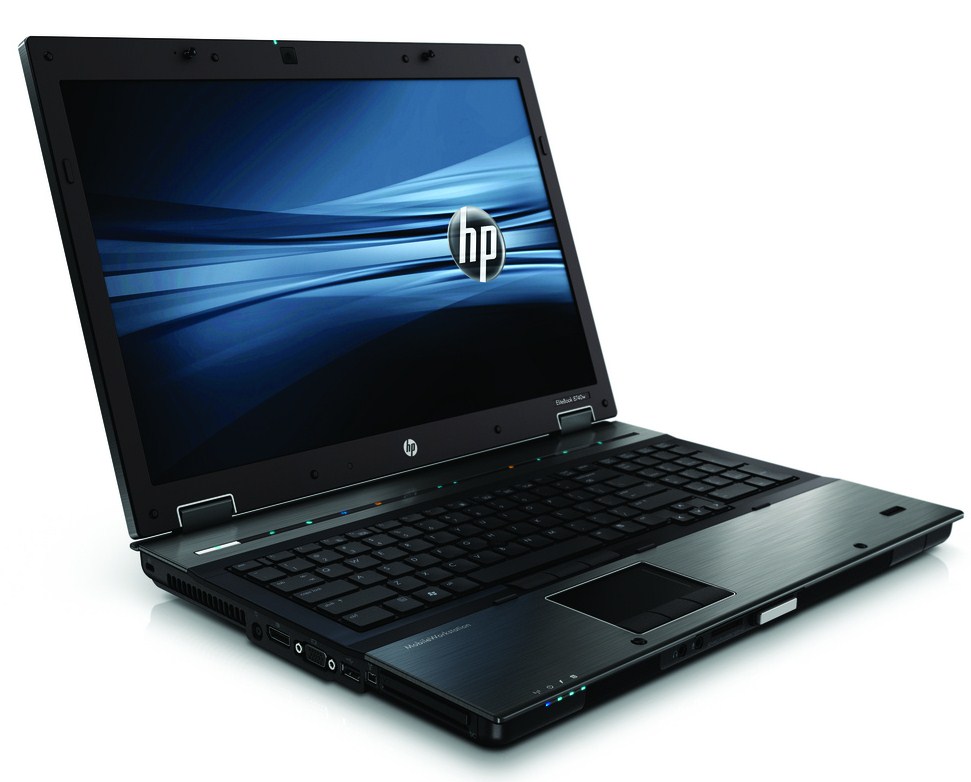
HP today unveiled workstation offerings that include the first small form factor workstation to be available in every region of the world, multicore processor updates to its Z Workstation series and a mobile workstation with DreamColor display technology.

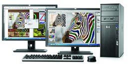
Adding to the award-winning HP Z Workstation series, the HP Z200 SFF Workstation delivers workstation performance and reliability in a sleek, ultracompact and affordable package, and is a great choice for space-constrained environments including the health care, engineering, education, financial and original equipment manufacturer markets.

Intel Introduces 2010 Core i7 Extreme, and Most Secure Data Center Processors

Combining unprecedented security, performance and energy efficiency, Intel Corporation today launched the Intel Xeon Processor 5600 series. The new processors deliver two new security features -- Intel Advanced Encryption Standard New Instructions (Intel AES-NI), and Intel Trusted Execution Technology (Intel TXT) -- that enable faster encryption and decryption performance for more secure transactions and virtualized environments, providing data centers with a stronger foundation for cloud security.

These are also the first server and workstation chips based on the groundbreaking, new Intel 32nm logic technology, which uses Intel's second-generation high-k metal gate transistors to increase speed and decrease energy consumption. The Intel Xeon Processor 5600 series supports up to six cores per processor and delivers up to 60 percent greater performance than the 45nm Intel Xeon processor 5500 series. In addition, data centers can replace 15 single-core servers with a single new one, and achieve a return on their investment in as little as 5 months.

BIOSTAR Introduces the TH55B HD Motherboard

Followed by Intel recent 32nm "Clarkdale" Core i5 / i3 processor launch with built-in GPU engine, it is now a brand new page and competition for all-in-one PC. BIOSTAR, a professional manufacturer of motherboards after its top-line H55 motherboards "TH55XE" being released, today we see another main stream board "TH55B HD" in the market remains high quality component design, outstanding over clocking capabilities and new colorful slots. And of course, it also offers more competitive prices.

"TH55B HD" - a member of BIOSTAR famous "T-Series" with Micro ATX form factor design, black color PCB, and supporting latest Intel 32nm "Clarkdale" Core i5 / i3 processor.

MSI X58 Mainboards Provide Full Support to Intel 32nm, 6-core LGA1366 Processors

In order to provide consumers more comprehensive upgrade services, MSI, the world-leading mainboard and graphic card manufacturer, announced today that all MSI mainboards using Intel X58 chipset are available for simple BIOS upgrade without reconfiguring any hardware settings to support the next-generation Intel 32nm CPUs. This will bring greater scalability to consumers and mark out the thoughtful upgrade consideration of MSI products right in the beginning of product design.

In addition to process advancement, lower operating temperature and higher performance, the new 32nm Intel processors are the first series that includes native 6-core products on the market. The multi-tasking performance provide by the new 32nm Intel processors will bring consumers the experience of extreme performance. The MSI X58 mainboards have been a heat on the market since they were launched for their outstanding specifications and performance. Another heat is expected from them for their full support and compatibility with the next-generation 32nm processors from Intel. And they will surely be the right choice for power users who dare to challenge the extremes.

MSI Releases High C/P Value H57/H55 Series Mainboards

World-renowned mainboard and graphics card manufacturer, MSI, today officially released H57/H55 Intel chipset products that offer outstanding performance, effective heat dissipation and remarkable power efficiency and stability. After installation of the 32nm Intel Core i5 and Core i3 processors with graphics cores integrated, ultra-strong display performance and outstanding multi-display capability complement MSI's exclusive OC Genie one-second overclocking technology. This enhances 3D performance by up to 45%, allowing smooth BD movie playback, and seize the advantage while gaming.

MSI H57/H55 Series mainboards with built-in industry leading OC Genie auto overclocking technology: Just press the OC Genie button on the mainboard and within one second; enjoy auto overclocking and an optimized processor. Memory module and chipset setting values give overall 3D performance a boost of up to 45%. Whether users want to watch a high bit-rate HD movie or go online for some head-to-head gaming, both can be enjoyed with image performance that is smoother and lag-free.

ASUS X58 Motherboards First to Support Upcoming 32 nm CPUs

ASUS announced that it is ready to support the upcoming 32nm processor based on the LGA1366 socket and the Intel X58 chipset. This next-generation 32nm infrastructure, supporting six multi-cores, will deliver maximum performance to ASUS X58-based motherboards via a comprehensive BIOS upgrade. Chie-Wei Lin, General Manager of ASUS Motherboard Business said, "This new processor architecture accommodates up to six cores and significantly improves CPU performance. By enabling the architecture in our award-winning X58-based motherboards, we can deliver one of the fastest personal computing platforms in history and we are very excited about it."

ASUS' entire range of X58-based motherboards is ready for the new 32nm processor. For maximum CPU performance and advanced graphics processing enabled by the six cores, users simply need to update the BIOS of their existing X58-based motherboards.

Toshiba Launches Highest Density Embedded NAND Flash Memory Devices

Toshiba Corp. (Toshiba) and Toshiba America Electronic Components, Inc. (TAEC), its subsidiary in the Americas, today announced the launch of a 64 gigabyte (GB) embedded NAND flash memory module, the highest capacity yet achieved in the industry. The chip is the flagship device in a line-up of six new embedded NAND flash memory modules that offer full compliance with the latest e-MMC standard, and that are designed for application in a wide range of digital consumer products, including Smartphones, mobile phones, netbooks and digital video cameras. Samples of the 64GB module are available from today, and mass production will start in the first quarter of 2010.

The new 64GB embedded device combines sixteen pieces of 32Gbit (equal to 4GB) NAND chips fabricated with Toshiba's cutting-edge 32nm process technology, and also integrates a dedicated controller. Toshiba is the first company to succeed in combining 16 pieces of 32Gbit NAND chips, and applied advanced chip thinning and layering technologies to realize individual chips that are only 30 micrometers thick. Full compliance with the JEDEC/MMCA Version 4.4(V4.4) standard for embedded MultiMediaCards supports standard interfacing and simplifies embedding in products, reducing development burdens on product manufacturers. Toshiba offers a comprehensive line-up of single-package embedded NAND Flash memories in densities ranging from 2GB to 64GB. All integrate a controller to manage basic control functions for NAND applications, and are compatible with the latest e-MMC standard and its new features, including defining multiple storage areas and enhanced security features.

Intel Reports Strong Third-Quarter Results

Intel Corporation today reported third-quarter revenue of $9.4 billion. The company reported operating income of $2.6 billion, net income of $1.9 billion and earnings per share (EPS) of 33 cents.

"Intel's strong third-quarter results underscore that computing is essential to people's lives, proving the importance of technology innovation in leading an economic recovery," said Paul Otellini, Intel president and CEO. "This momentum in the current economic climate, plus our product leadership, gives us confidence about our business prospects going forward. As we look ahead, Intel's game-changing 32nm process technology will usher in another wave of innovation from new, powerful Intel Xeon server platforms to high-performance Intel Core processors to low-power Intel Atom processors."

Highlights include:
  • Third-Quarter Revenue $9.4 Billion, Strongest Second-to-Third-Quarter Growth in over 30 years
  • Gross Margin 58 Percent, Up 7 Points Sequentially
  • Operating Income $2.6 Billion
  • Net Income $1.9 Billion
  • EPS 33 Cents
To read the complete earnings release, visit this page.

GLOBALFOUNDRIES To Highlight 32nm/28nm Technology Leadership at GSA Expo

As the semiconductor industry begins its transition to the next technology node, GLOBALFOUNDRIES is on track to take its position as the foundry technology leader. On October 1 at the Global Semiconductor Alliance Emerging Opportunities Expo & Conference in Santa Clara, Calif., GLOBALFOUNDRIES (Booth 321) will provide the latest details on its technology roadmap for the 32nm/28nm generations and its innovative "Gate First" approach to building transistors based on High-K Metal Gate (HKMG) technology.

"With each new technology generation, semiconductor foundries are increasingly challenged with the economics to sustain R&D and the know-how to bring these technologies to market in high-volume," said Len Jelinek, director and chief analyst, iSuppli. "With a heritage of rapidly ramping leading-edge technologies to high volumes at mature yields, combined with aggressive investments in capacity and technology, GLOBALFOUNDRIES is uniquely-positioned to challenge for next-generation foundry leadership."

Toshiba Adds 32 nm mSATA and Half-slim Solid State Drive Modules

Toshiba America Electronic Components, Inc. (TAEC), a U.S. marketing arm of Toshiba Corporation for electronic components, today announced a series of solid state drive (SSD) modules using the latest generation Toshiba 32nm MLC NAND flash, at Intel Developers Forum 2009. The Toshiba SG2 modules are offered in two types, one based on the new low-profile mini-SATA (mSATA) interface standard and the other a Half-Slim type, which uses a SATA connector. The drives are available in 30GB1 and 62GB modules. Volume production will start in October.

The two types of modules, each smaller than a business card, provide greater design flexibility and save space and cost compared to SSDs with hard disk drive form factors and cases. The 62GB module is only one seventh the volume and one eighth the weight of a 2.5-inch form factor SSD, and consumes half the power. With interface speeds up to 3 gigabits per second (Gb/s), a maximum sequential read speed of 180 megabytes per second (MBps)3,4 and a maximum sequential write speed of 70MBps,3,4 the modules will help bring the performance advantages of SSDs to notebooks, portable electronics and embedded systems. An advanced controller features a translation mode, which enables any drive configuration, and the drive supports 28-bit LBA (Logical Block Address) mode commands and 48-bit LBA mode commands. Multi-word DMA, Ultra-DMA modes and Advanced PIO commands are supported. The drives have an optional capability for secure Full Disk Encryption (FDE) backup that prevents unauthorized data access.

Intel to Invest $7 Billion in U.S. Manufacturing Facilities

Intel President and CEO Paul Otellini today announced the company would spend $7 billion over the next two years to build advanced manufacturing facilities in the United States. The investment funds deployment of Intel's industry-leading 32 nanometer (nm) manufacturing technology that will be used to build faster, smaller chips that consume less energy. The commitment represents Intel's largest-ever investment for a new manufacturing process.

Intel Developing Clarkdale to Replace Havendale Desktop Dual-Core Chip

On the course of coming up with mainstream derivatives of the Nehalem architecture, for Intel, there seems to be a big deal of uncertainty surrounding the dual-core parts. Havendale (desktop) and Auburndale (notebook) were stated by initial company road-maps as the company's dual-core chips. Later, news emerged of Intel reportedly scrapping both chips to find a 32 nm replacement in another chip codenamed Arrandale. In the latest company-slide exposé by VR-Zone, details emerge of yet another iteration to Intel's plans: Clarkdale. Correct spelling is Clarkdale and Arrandale by the way (not Clarksdale or Arandale).

While it is unclear at this point, if this chip, like the Arrandale (32 nm CPU + 32 nm IGP), is built to be deployed on both desktop and mobile platforms, the reason behind its development gains clarity. The Ibex-Peak platform design by Intel, be it dual-core or quad-core, consists of a standard multi-chip module (MCM)-based design, where two dice populate a package: the central processor, and the northbridge. The design gives the company flexibility by introducing a degree of modularity. After scrapping plans of a full-on processor built on the 45 nm high-K manufacturing process, Intel seems to have realised that its foundries won't be able to cater to many designs based on the 32 nm process initially, at once. Taking advantage of the MCM design, Intel is working on this new chip: Clarkdale, which consists of the processor die built on the 32 nm second-generation high-K process, with the northbridge being built on the existing 45 nm process. This design helps evade the manufacturing constraints Intel might have initially. The northbridge die will feature an integrated graphics processor that connects to its output using the flexible-display interface. With this, Intel is looking to bring in immediate and cost-cutting to the extant feasible.

Intel 32 nm Silicon Technology On Course for Late 2009

Having reacted rather sharply to the ongoing global economic slump by planning massive workforce and production cuts, one would expect Intel to be conservative with its development potential. In a contradiction to just that, a recent conversation EETimes had with Mark Bohr, director of Intel's technology and manufacturing group, the director said that the company is on course with its plans to introduce the newer 32 nm silicon fabrication technology by late 2009.

"The 32 nm technology is getting ready to go into the manufacturing phase, we are lining up fabs to support it and we expect great demand. We are on track for shipping products in the fourth quarter and have 22 nm technology in development for 2011" said Mr. Bohr. The conversation previewed some of the papers Intel plans to present at the International Solid-State Circuits Conference that convenes next week.

Intel follows a "tick-tock" model of product development cycle, wherein, the company designs new microprocessor designs and silicon fabrication technologies in alternation. In each cycle, an architecture gets to be made on at least two successive fabrication technologies before itself being succeeded by a newer design. Currently Intel employs the 45 nm High-K metal gate manufacturing technology, on which it introduced later variants of the Core 2 series CPUs, and has introduced its Nehalem architecture, with Core i7 being its first commercial implementation.

Intel Scraps 45 nm Nehalem Dual-Core Chips, Plans Replacement

Grappling with a deteriorating world economy, and overstocked inventories with current-generation Core 2 platforms, Intel seems to have had a change of plans with regards to its dual-core Nehalem-derivatives. Company roadmaps originally pointed at two chips, codenamed Havendale and Auburndale to be the dual-core MCM implementations of the Nehalem architecture, for desktops and notebooks respectively. The "MCM" (multi-chip module) part comes to light in the way the chips were originally conceived: two dice on a package, one holding the CPU complex and the other holding the northbridge, consisting of a memory controller, PCI-Express root complex, and a graphics controller.

Theo Valich, noted industry commentator, in his latest blog post in Theo's Bright Side of IT, mentions that Intel scrapped Havendale and Auburndale in its conceived form. The two were set to make possible Intel Core i4 and i3 SKUs. Instead, Intel is working to push forward the launch of their common successor by six months: the Arandale core. Arandale features in the future series of Nehalem-derived processors to be built on the 32nm high-K silicon process, slated for 2010. Arandale from all that is known thus far is the dual-core Nehalem implementation on 32nm lithography, apart from speculation of it holding a higher amount of L3 cache: possibly 6 MB against 4 MB on the Havendale/Auburndale. The Arandale core was originally slated for "back to school" season, 2010 (around September~October). After rescheduling the launch, it could arrive by March.

Intel Completes Next Generation, 32nm Process Development Phase

Intel Corporation has completed the development phase of its next-generation manufacturing process that further shrinks chip circuitry to 32 nanometers (a billionth of a meter). The company is on track for production readiness of this future generation using even more energy-efficient, denser and higher performing transistors in the fourth quarter of 2009. Intel will provide a multitude of technical details around the 32nm process technology along with several other topics during presentations at the International Electron Devices meeting (IEDM) next week in San Francisco.

ARM, Chartered, IBM and Samsung Collaborate to Enable 32nm and 28nm Systems-on-Chip

IBM, Chartered Semiconductor Manufacturing, Samsung Electronics, and ARM today announced they will develop a comprehensive 32 nanometer (nm) and 28nm Systems-on-a-Chip (SoCs) design platform based on high-k metal-gate (HKMG) technology from the IBM-led joint-development alliance. Under this multi-year collaboration, ARM will develop and license a design platform of physical intellectual property (IP) including logic, memory and interface products for the Common Platform technology alliance of IBM, Chartered and Samsung for distribution to their customers.

IBM and AMD First to Reach the 22 nm Silicon Fabrication Mark

IBM and its chip development partners announced today that they've developed the first functional 22nm silicon fabricated SRAM cell. This puts them ahead of Intel, which had announced its technological entry into the 32 nm domain in September, 2007. SRAM is usually the first semiconductor device a chip-maker tests a new fabrication-process on, before working on microprocessors. These devices were developed and manufactured by AMD, Freescale, IBM STMicroelectronics, Toshiba and the College of Nanoscale Science and Engineering (CNSE). They were built in the conventional 6-transistor design and on a 300 mm wafer. This level of miniaturization made the SRAM cell shrink to a mere 0.1 sq. μm, compare this to the SRAM cells that go into making caches on the 45 nm Intel processors, 0.346 sq. μm.

TSMC Outlines New High-k/Metal-gate 32nm Process

Responding to IBM and its development partners that took the lead in the nm battle by announcing the availability of a high-k and metal-gate 32nm offering, Taiwan Semiconductor Manufacturing (TSMC) today outlined more details about its 32nm process. Rick Tsai, president and chief executive of the company said "We will have high-k and metal-gate at 32nm," during a keynote at the 2008 Technology Symposium. Jack Sun, vice president of research and development, also indicated that TSMC will develop a third-generation triple-gate oxide technology for its 32nm low-power process. For its 32nm high-performance process, TSMC will offer a high-k and metal gate technology, Sun added.

IBM and Other Development Partners Deliver Major Semiconductor Performance Leap

IBM and its joint development partners - Chartered Semiconductor Manufacturing, Freescale, Infineon Technologies AG, Samsung Electronics, STMicroelectronics N.V. and Toshiba Corporation - today announced that they have collectively demonstrated significant performance and power consumption advantages over industry standards by using a breakthrough material known as "high-k/metal gate" (HKMG) on silicon manufactured at IBM's state-of-art 300 millimeter (mm) semiconductor fabrication facility in East Fishkill, N.Y. With this achievement the joint development partners are now ready for early customer engagements.
Return to Keyword Browsing
Apr 19th, 2024 01:49 EDT change timezone

New Forum Posts

Popular Reviews

Controversial News Posts