News Posts matching #3nm

Return to Keyword Browsing

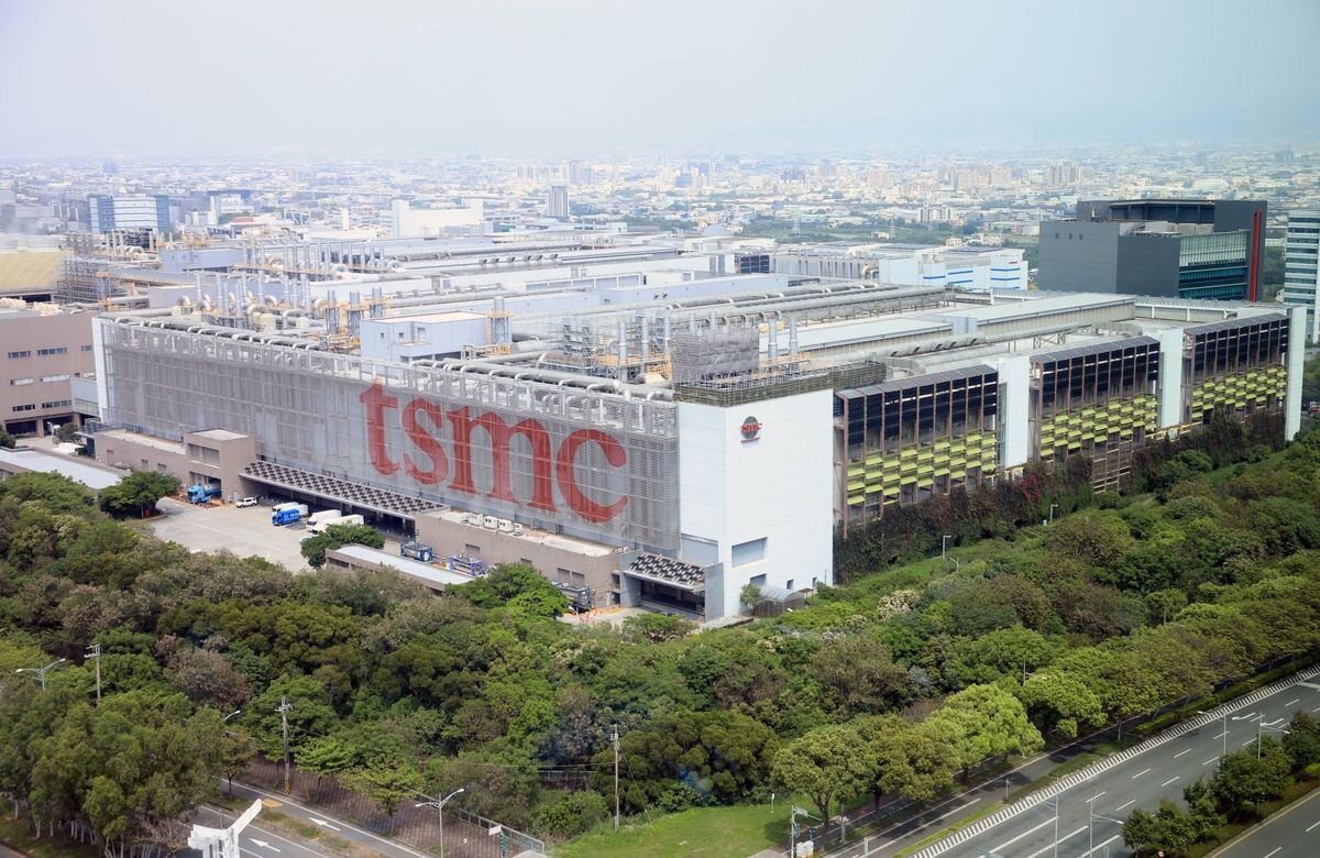
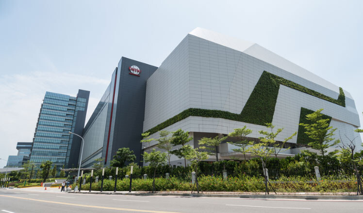
TSMC 3nm Node to Make 20% of Company's Revenues in 2024

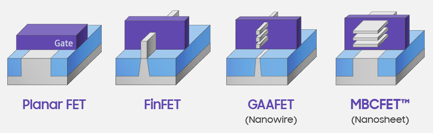
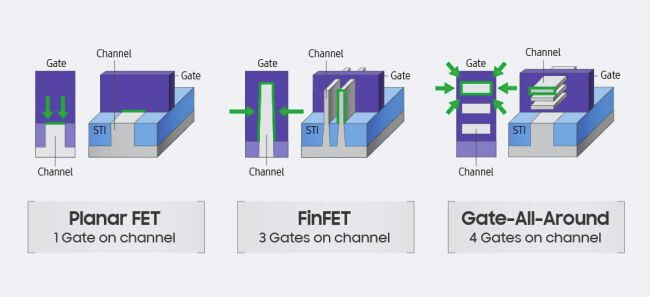
The 3 nm EUV node, which will be TSMC's final semiconductor fabrication node to implement FinFET transistors, will make for a staggering 20% of TSMC's revenues in 2024, a report by ICSmart says. 20% is big for a new foundry node, considering that TSMC is simultaneously running 4 nm and 5 nm EUV nodes; 6 nm and 7 nm DUV nodes; and several older mature nodes. Apple is expected to be the foundry's biggest customer for 3 nm, as it could power the company's current A17 and M3, and upcoming A18 and M4 line of chips for its next-generation iPhone and MacBooks; followed by NVIDIA, AMD, and possibly even Intel. AMD is expected to build some versions of its upcoming "Zen 5" processors on 3 nm; while Intel is expected to use 3 nm for some of the tiles of its upcoming "Lunar Lake" processor. The same report goes to suggest that 3 nm will make up 30% of TSMC's revenues in 2025.

Global Top 10 Foundries Q4 Revenue Up 7.9%, Annual Total Hits US$111.54 Billion in 2023

The latest TrendForce report reveals a notable 7.9% jump in 4Q23 revenue for the world's top ten semiconductor foundries, reaching $30.49 billion. This growth is primarily driven by sustained demand for smartphone components, such as mid and low-end smartphone APs and peripheral PMICs. The launch season for Apple's latest devices also significantly contributed, fueling shipments for the A17 chipset and associated peripheral ICs, including OLED DDIs, CIS, and PMICs. TSMC's premium 3 nm process notably enhanced its revenue contribution, pushing its global market share past the 60% threshold this quarter.

TrendForce remarks that 2023 was a challenging year for foundries, marked by high inventory levels across the supply chain, a weak global economy, and a slow recovery in the Chinese market. These factors led to a downward cycle in the industry, with the top ten foundries experiencing a 13.6% annual drop as revenue reached just $111.54 billion. Nevertheless, 2024 promises a brighter outlook, with AI-driven demand expected to boost annual revenue by 12% to $125.24 billion. TSMC, benefiting from steady advanced process orders, is poised to far exceed the industry average in growth.

Intel, Marvell, and Synopsys to Showcase Next-Gen Memory PHY IP Capable of 224 Gbps on 3nm-class FinFET Nodes

The sneak peeks from the upcoming IEEE Solid State Circuit Conference continues, as the agenda items unveil interesting tech that will be either unveiled or demonstrated there. Intel, Synopsys, and Marvell, are leading providers of DRAM physical layer interface (PHY) IP. Various processor, GPU, and SoC manufacturers license PHY and memory controller IP from these companies, to integrate with their designs. All three companies are ready with over 200 Gbps around the 2.69 to 3 petajoule per bit range. This energy cost is as important as the data-rate on offer; as it showcases the viability of the PHY for a specific application (for example, a smartphone SoC has to conduct its memory sub-system at a vastly more constrained energy budget compared to an HPC processor).

Intel is the first in the pack to showcase a 224 Gbps sub-picojoule/bit PHY transmitter that supports PAM4 and PAM6 signaling, and is designed for 3 nm-class FinFET foundry nodes. If you recall, Intel 3 will be the company's final FinFET node before it transitions to nanosheets with the Intel 20A node. At the physical layer, all digital memory signal is analogue, and Intel's IP focuses on the DAC aspect of the PHY. Next up, is a somewhat similar transceiver IP by Synopsys. This too claims 224 Gbps speeds at 3 pJ/b, but at a 40 dB insertion loss; and is designed for 3 nm class FinFET nodes such as the TSMC N3 family and Intel 3. Samsung's 3 nm node uses the incompatible GAAFET technology for its 3 nm EUV node. Lastly, there's Marvell, with a 212 Gb/s DSP-based transceiver for optical direct-detect applications on the 5 nm FinFET nodes, which is relevant for high speed network switching fabrics.

DNP Develops Photomask Process for 3nm EUV Lithography

Dai Nippon Printing Co., Ltd. (DNP) has successfully developed a photomask manufacturing process capable of accommodating the 3-nanometer (10-9 meter) lithography process that supports Extreme Ultra-Violet (EUV) lithography, the cutting-edge process for semiconductor manufacturing.

Background
DNP has continually responded to the demands of semiconductor manufacturers in terms of performance and quality. In 2016, we became the world's first merchant photomask manufacturer to introduce the multi-beam mask writing tool (MBMW). In 2020, we developed a photomask manufacturing process for 5 nm EUV lithography processes, and have been supplying masks that meet the needs of the semiconductor market. In this latest development, in order to meet the needs of further miniaturization, we have developed a photomask for EUV lithography capable of supporting 3 nm processes.

Apple Unveils New M3, M3 Pro, and M3 Max Processors on TSMC 3nm

Apple today announced M3, M3 Pro, and M3 Max, three chips featuring groundbreaking technologies that deliver dramatically increased performance and unleash new capabilities for Mac. These are the first personal computer chips built using the industry-leading 3-nanometer process technology, allowing more transistors to be packed into a smaller space and improving speed and efficiency. Together, M3, M3 Pro, and M3 Max show how far Apple silicon for the Mac has come since the debut of the M1 family of chips.

The M3 family of chips features a next-generation GPU that represents the biggest leap forward in graphics architecture ever for Apple silicon. The GPU is faster and more efficient, and introduces a new technology called Dynamic Caching, while bringing new rendering features like hardware-accelerated ray tracing and mesh shading to Mac for the first time. Rendering speeds are now up to 2.5x faster than on the M1 family of chips. The CPU performance cores and efficiency cores are 30 percent and 50 percent faster than those in M1, respectively, and the Neural Engine is 60 percent faster than the Neural Engine in the M1 family of chips. And, a new media engine now includes support for AV1 decode, providing more efficient and high-quality video experiences from streaming services. The M3 family of chips continues the tremendous pace of innovation in Apple silicon, and brings massive enhancements and new features to the new MacBook Pro and iMac.

Samsung's 3 nm GAA Process Identified in a Crypto-mining ASIC Designed by China Startup MicroBT

Semiconductor industry research firm TechInsights said it has found that Samsung's 3 nm GAA (gate-all-around) process has been incorporated into the crypto miner ASIC (Whatsminer M56S++) from a Chinese manufacturer, MicroBT. In a Disruptive Technology Event Brief exclusively provided to DIGITIMES Asia, TechInsights points out that the significance of this development lies in the commercial utilization of GAA technology, which facilitates the scaling of transistors to 2 nm and beyond. "This development is crucial because it has the potential to enhance performance, improve energy efficiency, keep up with Moore's Law, and enable advanced applications," said TechInsights, identifying the MicroBT ASIC chip the first commercialized product using GAA technology in the industry.

But this would also reveal that Samsung is the foundry for MicroBT, using the 3 nm GAA process. DIGITIMES Research semiconductor analyst Eric Chen pointed out that Samsung indeed has started producing chips using the 3 nm GAA process, but the capacity is still small. "Getting revenues from shipment can be defined as 'commercialization', but ASIC is a relatively simple kind of chip to produce, in terms of architecture."

Samsung Claims Higher 3 nm Yields than TSMC

Competition between Samsung and TSMC in the 4 nm and 3 nm foundry process markets is about to heat up, with the Korean foundry claiming yields competitive to those of TSMC, according to a report in the Kukmin Ilbo, a Korean daily newspaper. 4 nm is the final silicon fabrication process to use the FinFET technology that powered nodes ranging between 16 nm to 4 nm. Samsung Foundry is claiming 4 nm wafer yields of 75%, against the 80% yields figure put out by TSMC. 4 nm powers several current-generation mobile SoCs, PC processors, and more importantly, the GPUs driving the AI gold-rush.

Things get very interesting with 3 nm, the node that debuts GAA-FET (gates all around FET) technology. Here, Samsung claims to offer higher yields than TSMC, with its 3 nm GAA node clocking 60% yields, against 55% put out by TSMC. Samsung was recently bitten by a scandal where its engineers allegedly falsified yields figures to customers to score orders, which had a cascading effect on the volumes and competitiveness of their customers. We're inclined to think that Samsung has taken lessons and is more careful with the yields figures being reported in the press. Meanwhile, Intel Foundry Services competes with the Intel 3 node, which is physically 7 nm FinFET, but with electrical characteristics comparable to those of 3 nm.

One of TSMC's Biggest Customers Cuts 3nm Wafer Orders As Consumer Demand Deflates

A major unnamed customer of TSMC has reportedly cut their order for 3 nm wafers. Foundry customers usually place orders for cutting-edge foundry nodes several quarters in advance, in exchange for priority foundry allocations, and preferential rates, while foundries use revenues from these orders to develop the capacity for manufacture these chips. The 3 nm customer could be anyone—Qualcomm, Mediatek, NVIDIA, AMD, or Intel. Order cancellations have reportedly had a domino-effect on the upstream supply-chain of TSMC, hitting suppliers of raw materials, manufacturing equipment, and other consumables. There is an industry-wide slump in demand for consumer electronics and PC hardware, which reflects in the slump in revenues and/or guidance in quarterly financial results releases by prominent companies.

TSMC Announces the N3 FinFlex, N3E, and N2 Nodes, and 3DFabric

TSMC today showcased the newest innovations in its advanced logic, specialty, and 3D IC technologies at the Company's 2022 North America Technology Symposium, with the next-generation leading-edge N2 process powered by nanosheet transistors and the unique FINFLEX technology for the N3 and N3E processes making their debut.

Resuming as an in-person event after being held online in the past two years, the North America symposium in Santa Clara, California, kicks off a series of Technology Symposiums around the world in the coming months. The Symposiums also feature an Innovation Zone that spotlights the achievements of TSMC's emerging start-up customers.

Intel and TSMC Strike 3nm Deal, New Hsinchu Fab to Cater to Intel

It looks like Intel and TSMC have a deal in place to manufacture 3 nm chips. The world-leading Taiwanese fab is setting up a new facility exclusively to cater to Intel, according to DigiTimes, citing industry sources. This facility will be located in the Baoshan area of Hsinchu, in northern Taiwan. The 3 nm node will enable Intel to keep its newfound cadence of launching new CPU microarchitectures with IPC increases each year. The annual IPC increase cadence in particular, would be faster than even the "Tick-Tock" cadence prior to 2015, as the company pushed IPC increases and foundry nodes each alternating year. The company faces stiff competition from AMD, which has been posting IPC increases each year since 2017, and leveraged TSMC 7 nm nodes to beat Intel in the IPC game for the first time in over 17 years.

Intel Negotiates 3nm Allocation with TSMC Even as Pat Gelsinger Cautions Against Investing in Taiwan

Intel is reportedly in talks with TSMC to secure foundry allocation to meet its product roadmap execution. The company is sending an executive delegation to meet with TSMC later this month, to secure foundry capacity for the N3 (3 nm) silicon fabrication node, and ensure that Intel's allocation isn't affected by other customers such as Apple. As part of its IDM 2.0 strategy, Intel has decided to build its products essentially as multi-chip modules with each block of IP built on a silicon fabrication node most optimal to it, so the company maximizes cutting-edge foundry nodes only on the technology that benefits from it the most. N3 will play a vital role with logic/compute tiles in products bound for 2023, as N3 hits critical volume in the first half of the year.

In related news, Intel CEO Pat Gelsinger speaking at the Fortune Brainstorm Tech conference, stressed on the importance for American chip designers to seek out semiconductor manufacturing in America, and cautioned against investing in Taiwan (without naming TSMC). This comes in the wake of geopolitical uncertainty in the region. In response to this statement issued to DigiTimes, TSMC CEO Mark Liu downplayed the matter, and said that Gelsinger's statement wasn't worth responding to, and that he doesn't slander industry colleagues. TSMC and Samsung have each announced multi-billion Dollar foundry investments in the US, in attempts to make the global semiconductor supply chains resilient to any security situation that may emerge in East Asia.

Samsung Foundry Announces GAA Ready, 3nm in 2022, 2nm in 2025, Other Speciality Nodes

Samsung Electronics, a world leader in advanced semiconductor technology, today unveiled plans for continuous process technology migration to 3- and 2-nanometer (nm) based on the company's Gate-All-Around (GAA) transistor structure at its 5th annual Samsung Foundry Forum (SFF) 2021. With a theme of "Adding One More Dimension," the multi-day virtual event is expected to draw over 2,000 global customers and partners. At this year's event, Samsung will share its vision to bolster its leadership in the rapidly evolving foundry market by taking each respective part of foundry business to the next level: process technology, manufacturing operations, and foundry services.

"We will increase our overall production capacity and lead the most advanced technologies while taking silicon scaling a step further and continuing technological innovation by application," said Dr. Siyoung Choi, President and Head of Foundry Business at Samsung Electronics. "Amid further digitalization prompted by the COVID-19 pandemic, our customers and partners will discover the limitless potential of silicon implementation for delivering the right technology at the right time."

Applied Materials Breakthrough in Chip Wiring Enables Logic Scaling to 3nm and Beyond

Applied Materials, Inc. today unveiled a new way to engineer the wiring of advanced logic chips that enables scaling to the 3 nm node and beyond. While size reduction benefits transistor performance, the opposite is true in the interconnect wiring: smaller wires have greater electrical resistance which reduces performance and increases power consumption. Without a materials engineering breakthrough, interconnect via resistance would increase by a factor of 10 from the 7 nm node to the 3 nm node, negating the benefits of transistor scaling.

Applied Materials has developed a new materials engineering solution called the Endura Copper Barrier Seed IMS. It is an Integrated Materials Solution that combines seven different process technologies in one system under high vacuum: ALD, PVD, CVD, copper reflow, surface treatment, interface engineering and metrology. The combination replaces conformal ALD with selective ALD, eliminating a high-resistivity barrier at the via interface. The solution also includes copper reflow technology that enables void free gap fill in narrow features. Electrical resistance at the via contact interface is reduced by up to 50 percent, improving chip performance and power consumption, and enabling logic scaling to continue to 3 nm and beyond.

TSMC to Roll Out 3nm Plus Manufacturing Process in 2023

The possibility barely exists to account for all the silicon manufacturing processes currently in development; TSMC themselves are rolling out 5 nm, 4 nm, 3 nm, and 2 nm processes at various points in time in the future. Now, the company has announced that it will be rolling out a revision of the 3 nm manufacturing process, named 3 nm Plus, come 2023. According to DigiTimes, the Taiwanese manufacturer's first client for this process will be Apple.

There is no information on what exactly 3 nm Plus leverages and offers over the "vanilla" 3 nm process. It could be anything from higher transistor density, lower power consumption, or higher operating frequency - or maybe a mixture of the three. The original 3 nm manufacturing process is set to offer a 15% performance gain over the current top-of-the-line 5 nm node, with 30% decreased power use and up to 70% density increase. Interestingly, TSMC is keeping their FinFet manufacturing technology, on grounds of better implementation costs and higher power efficiency compared to the more exotic GAA (Gate-All-Around) technology that its rival Samsung, for one, aims to implement in 3 nm.

TSMC Details 3nm N3, 5nm N5, and 3DFabric Technology

TSMC on Monday kicked off a virtual tech symposium, where it announced its new 12 nm N12e node for IoT edge devices, announced the new 3DFabric Technology, and detailed progress on its upcoming 5 nm N5 and 3 nm N3 silicon fabrication nodes. The company maintains that the N5 (5 nm) node offers the benefits of a full node uplift over its current-gen N7 (7 nm), which recently clocked over 1 billion chips shipped. The N5 node incorporates EUV lithography more extensively than N6/N7+, and in comparison to N7 offers 30% better power at the same performance, 15% more performance at the same power, and an 80% increase in logic density. The company has commenced high-volume manufacturing on this node.

2021 will see the introduction and ramp-up of the N5P node, an enhancement of the 5 nm N5 node, offering a 10% improvement in power at the same performance, or 5% increase in performance at the same power. A nodelet of the N5 family of nodes, called N4, could see risk production in Q4 2021. The N4 node is advertised as "4 nm," although the company didn't get into its iso-power/iso-performance specifics over the N5 node. The next major node for TSMC will be the 3 nm N3 node, with massive 25%-30% improvement in power at the same performance, or 10%-15% improvement in performance at same power, compared to N5. It also offers a 70% logic density gain over N5. 3DFabric technology is a new umbrella term for TSMC's CoWoS (chip on wafer on substrate), CoW (chip on wafer), and WoW (wafer on wafer) 3-D packaging innovations, with which it plans to offer packaging innovations that compete with Intel's various new 3D chip packaging technologies on the anvil.

Samsung to Commence 5nm EUV Mass-Production in Q2-2020, Develop 3nm GAAFET Node

Samsung in its Q1-2020 financials release disclosed that the company will commence mass production of chips on its cutting-edge 5 nanometer EUV silicon fabrication process within Q2-2020 (that's before July 2020). This is big, as it lends credence to rumors of NVIDIA secretly developing 5 nm GPUs. Suddenly, it's possible that "Ampere," if not "Hopper," is 5 nm EUV-based, as NVIDIA has chosen Samsung to be its foundry partner for next-generation GPUs.

"In the second quarter, the Company aims to expand EUV leadership, beginning with the start of mass production of 5 nm products, while closely monitoring the uncertain market situation caused by COVID-19," the company states in the release. Samsung also announced that following commencement of mass production on 5 nm, further development of GAAFET (gate all-around FET) 3 nanometer silicon fabrication process will get underway. The company appears to be erring on the side of caution with its forward-looking statements, though. Much of what Samsung does will be dictated by the impact of COVID-19 on the supply chain and market.

TSMC 3nm Process Packs 250 Million Transistors Per Square Millimeter

Imagine being able to shrink a Pentium 4 processor die to the size of a pin-head (if you can figure out how to place 478 bumps on it). TSMC revealed that its future 3 nanometer silicon fabrication node has a development target of 250 million transistors per mm². Called N3, the next-generation silicon fabrication node succeeds TSMC's N5 family of 5 nm-class nodes (that's N5 and any possible refinements).

TSMC CEO CC Wei confirmed that development of the 3 nm node is on-track, with risk production scheduled for 2021 and volume production commencing in the second half of 2022. Perhaps the most startling revelation is that TSMC has decided to stick with FinFETs for N3 owing to the maturity of the technology. Experts are of the opinion that sub-5 nm nodes will require major innovations with materials and structures. TSMC claims that N3 will provide a 10-15% speed improvement at iso-power or 25-30% power reduction at iso-speed, compared to N5.

Intel Courts TSMC 6nm and 3nm Nodes for Future Xe GPU Generations

Intel is rumored to be aligning its future-generation Xe GPU development with TSMC's node development cycle, with the company reportedly negotiating with the Taiwanese foundry for 6 nm and 3 nm allocation for its large Xe GPUs. Intel's first Xe discrete GPUs for the market, however, are reportedly built on the company's own 10 nm+ silicon fabrication process.

While Intel's fascination with TSMC 3 nm is understandable, seeking out TSMC's 6 nm node raises eyebrows. Internally referred to as "N6," the 6 nm silicon fabrication node at TSMC is expected to go live either towards the end of 2020 or early 2021, which is when Intel's 10 nm+ node is expected to pick up volume production, beginning with the company's "Tiger Lake" processors. Perhaps a decision has been made internally to ensure that Xe doesn't eat too much into Intel's own foundry capacities meant for processor manufacturing, and to instead outsource Xe manufacturing to third-party foundries like TSMC and Samsung eventually. Way back in April 2019 it was rumored that Intel was evaluating Samsung as a foundry partner for Xe.

Samsung Announces Breakthrough in Building Blocks of 3nm Circuits, Updates Roadmap

Samsung Electronics Co., Ltd., a world leader in advanced semiconductor technology, today announced its ongoing commitment to foundry innovation and service at the Samsung Foundry Forum 2019 USA, providing the silicon community with wide-ranging updates on technology advances that support the most demanding applications of today and tomorrow.

The event, held today in Santa Clara, California, features top Samsung executives and industry experts reviewing progress on semiconductor technologies and foundry platform solutions that enable developments in artificial intelligence (AI), machine learning, 5G networking, automotive, the Internet of Things (IoT), advanced data centers and many other domains.

TSMC Cleared to Build New 3 nm Manufacturing Factory in Southern Taiwan

The world's largest contract semiconductor manufacturing company, TSMC, has been cleared to commence construction of a new 3 nm chip factory at the Southern Taiwan Science Park in Tainan. The new factory is expected to use 20 percent renewable energy and 50 percent recycled water.

The factory's environmental impact assessment was accepted by the Environmental Protection Administration (EPA) on Dec. 19, after concerns were raised about use of water and power sources. TSMC is expected to invest NT$600 million (US$19.45 million) in the project, with construction to begin in 2022. Production is planned to start in late 2022 or early 2023. At the same site, TSMC is also building a 5 nm chip factory, which is expected to be up and running in late 2019 or early 2020.

Samsung to Power Future High-Performance Computing and Connected Devices

Samsung Electronics, a world leader in advanced semiconductor technology solutions, today unveiled a series of new silicon innovations at the heart of future high-performance computing and connected devices. With comprehensive process technology roadmap updates down to 3-nanometer (nm) at the annual 'Samsung Foundry Forum (SFF) 2018 USA', Samsung Foundry is focused on providing customers with the tools necessary to design and manufacture powerful, yet energy-efficient system-on-chips (SoC) for a wide range of applications.

"The trend toward a smarter, connected world has the industry demanding more from silicon providers," said Charlie Bae, executive vice president and head of the Foundry Sales & Marketing Team at Samsung Electronics. "To meet that demand, Samsung Foundry is powering innovation at the silicon level that will ultimately give people access to data, analysis, and insight in new and previously unthought-of ways to make human lives better. It is imperative for us to accomplish the first-time silicon success for our customers' next-generation chip designs."
Return to Keyword Browsing
Apr 25th, 2024 12:15 EDT change timezone

New Forum Posts

Popular Reviews

Controversial News Posts