News Posts matching #6 nm

Return to Keyword Browsing

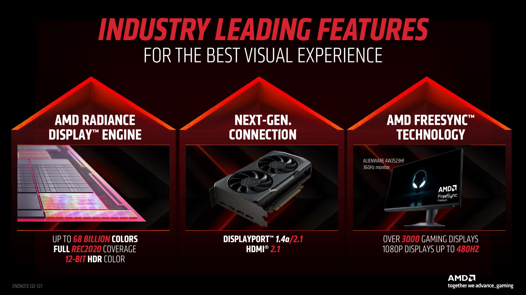
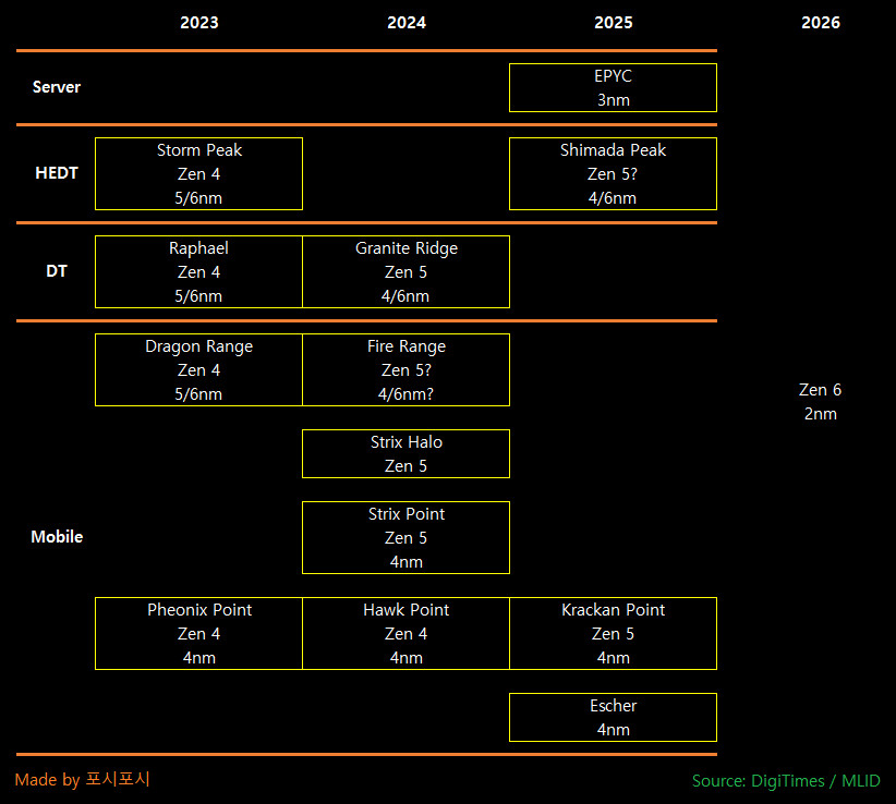
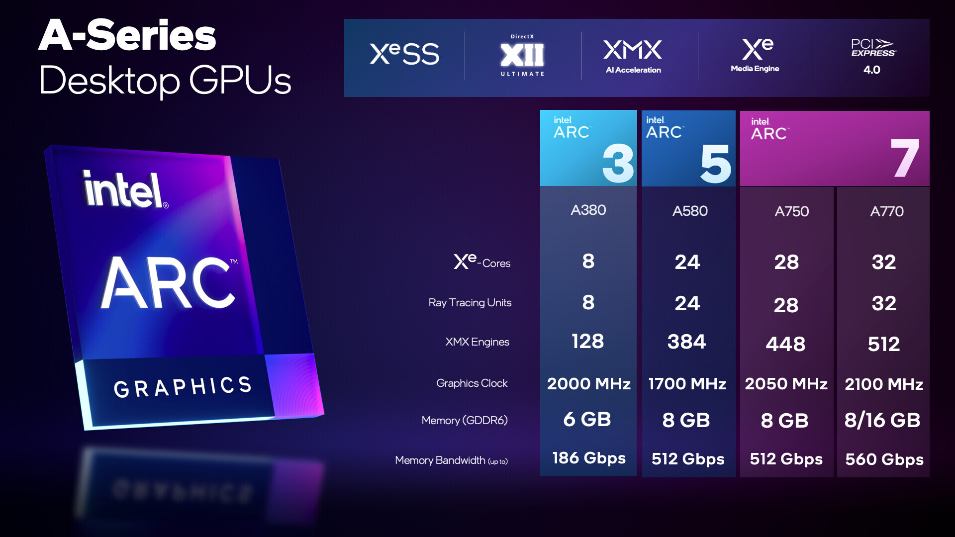
AMD Launches Radeon RX 7600 Graphics Card

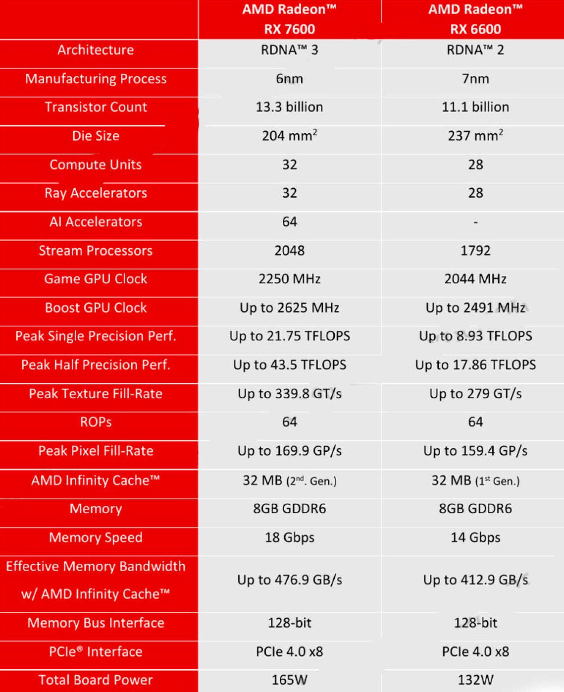
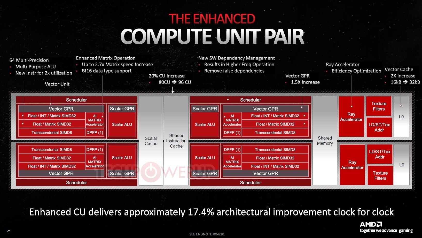
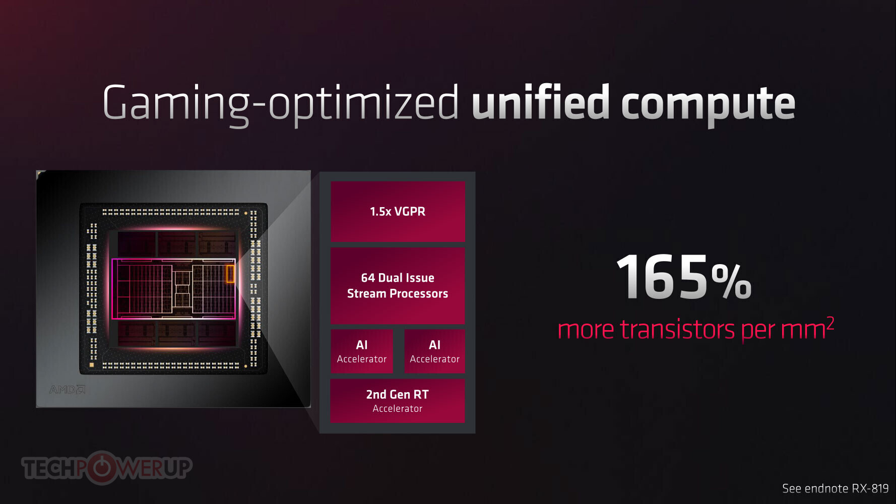
AMD today announced its Radeon RX 7600 graphics card, which competes against NVIDIA's upcoming RTX 4060, and succeeds the RX 6600. This GPU is based on the RDNA3 graphics architecture, but the "Navi 33" monolithic silicon it's based on, is built on the older 6 nm foundry node. The card has a total board power of 169 W, and draws power from a single 8-pin PCIe power connector. The RX 7600 maxes out this silicon, enabling all 2,048 stream processors, 64 AI Accelerators, 32 Ray Accelerators, 128 TMUs, and 64 ROPs. It offers 8 GB of memory, but using faster 18 Gbps memory chips, while the memory bus width remains 128-bit. The GPU comes with 32 MB of 2nd generation Infinity Cache memory. AMD is targeting the 1080p AAA gaming crowed with the RX 7600, with a starting price of USD $269.

AMD Reportedly Adjusts Radeon RX 7600 GPU MSRP to $269/€299

According to brand new information sent to the press and influencers yesterday, AMD has likely made a last minute change to its pricing strategy - VideoCardz has communicated with insider sources and confirms that an official email contains this message: "The Radeon RX 7600 will now be available starting at an SEP of $269 USD, beginning on May 25."

Industry experts were predicting a $299 MSRP for the upcoming Radeon RX 7600 graphics card lineup, based on possible earlier communications (under embargo) from AMD, but the company has seemingly decided to change its pricing strategy ($269/€299) only three days before the May 25 launch. Its monolithic RDNA 3 Navi 33 XL GPU (6 nm) is set to go head-to-head against NVIDIA's GeForce RTX 4060 Ti graphics card range later this week - the latter's specifications look to be superior according to leaked info - so Team Red could be making adjustments in order to stay competitive in the lower-end gaming-oriented GPU market.

AMD Radeon RX 7600 Final Specs and Power Figures Leaked, Uses 6 nm

Here are the final specifications of the Radeon RX 7600 RDNA3 graphics card, bound for launch later this month. The specs list springs up some surprises. To begin with, while the GPU at the heart of the RX 7600 is based on the latest RDNA3 graphics architecture, it is built on the older 6 nm (DUV) silicon fabrication process—the same one on which the previous "Navi 24" was based. The silicon has a transistor count of 13.3 billion, about 2 billion more than the 7 nm "Navi 23" Powering the RX 6600 series, but a die-size of 204 mm². The GPU has a PCI-Express 4.0 x8 host interface, and a 128-bit GDDR6 memory interface. As the RX 7600, it has a TBP (total board power) value of 165 W, which is over 30 W more than the RX 6600.

At this point, it's not known whether the RX 7600 maxes out the silicon it is based on. It gets 32 RDNA3 compute units (CU), which work out to 2,048 stream processors (with the same dual-issue instruction rate feature as the RX 7900 series); 32 Ray Accelerators, and 64 AI Accelerators. The GPU has 128 TMUs, and 64 ROPs. The GPU has 32 MB of second-generation Infinity Cache memory. The 8 GB of GDDR6 memory ticks at 18 Gbps, which over the 128-bit memory bus works out to 288 GB/s of memory bandwidth. AMD claims that when coupled with the on-die cache, the "effective bandwidth" is 476.9 GB/s. NVIDIA is putting out similar "effective" figures for its RTX 4060 series, so this could become a norm. The RX 7600 comes with a game frequency of 2250 MHz, and 2625 MHz boost. AMD is making 550 W as its PSU recommendation, compared to the 450 W it did for the RX 6600. The company considers the RX 7600 to be the logical successor of the RX 6600 (and neither the RX 6600 XT nor the RX 6650 XT).

AMD Ryzen 8000 "Granite Ridge" Zen 5 Processor to Max Out at 16 Cores

AMD's next-generation Ryzen 8000 "Granite Ridge" desktop processor based on the "Zen 5" microarchitecture, will continue to top out at 16-core/32-thread as the maximum CPU core-count possible, says a report by PC Games Hardware. The processor will retain the chiplet design of the current Ryzen 7000 "Raphael" processor, with two 8-core "Zen 5" CCDs, and one I/O die. It's very likely that AMD will reuse the same 6 nm client I/O die (cIOD) as "Raphael," just the way it used the same 12 nm cIOD between Ryzen 3000 "Matisse" and Ryzen 5000 "Vermeer;" but with updates that could enable higher DDR5 memory speeds. Each of the up to two "Eldora" Zen 5 CCDs has 8 CPU cores, with 1 MB of dedicated L2 cache per core, and 32 MB of shared L3 cache. The CCDs are very likely to be built on the TSMC 3 nm EUV silicon fabrication process.

Perhaps the most interesting aspect of the PCGH leak would have to be the TDP numbers being mentioned, which continue to show higher-performance SKUs with 170 W TDP, and lower tiers with 65 W TDP. With its CPU core-counts not seeing increases, AMD would bank on not just the generational IPC increase of its "Zen 5" cores, but also max out performance within the power envelope of the new node, by dialing up clock speeds. AMD could ride out 2023 with its Ryzen 7000 "Zen 4" processors on the desktop platform, with "Granite Ridge" slated to enter production only by Q1-2024. The company could update its product stack in the meantime, perhaps even bring the 4 nm "Phoenix" monolithic APU silicon to the Socket AM5 desktop platform. Ryzen 8000 is expected to retain full compatibility with existing Socket AM5, and AMD 600-series chipset motherboards.

MediaTek Announces Dimensity 8050 SoC, Seems to be a Rebadged Dimensity 1300/1200

MediaTek has been unveiling some new mobile chipsets this week, but keen-eyed news outlets have noticed that the Taiwanese fabless semiconductor company is simply renaming and relaunching hardware from last year, with some tweaks here and there. Today's announcement of the Dimensity 8050 SoC was almost immediately questioned - GSMArena noticed that this "new" model was a near dead ringer, in terms of specifications, for last year's mid-range Dimensity 1300 and 1200 smartphone chipsets. There are some upgrades in terms of memory bandwidth, and MediaTek boasts that the 8050 has been updated with its sixth generation HyperEngine technology.

Alarm bells were ringing when folks realized that the much older Dimensity 8000 SoC was built on a 5 nm process - the supposedly superior (in terms of model number hierarchy) 8005 is a 6 nm chip. Last week the mobile specialist site also spotted that MediaTek's Dimensity 7050 chipset was yet another example of the smartphone tech company rolling out a "rebranding phase." The news outlet pointed out that this newly revealed mobile CPU was just a renamed Dimensity 1080 - with the original model having hit the market in November 2022. MediaTek seems to renaming several older chipsets based on TSMC's 6 nm process - it is possible that this effort is part of a company drive to clear surplus silicon.

Report Suggests AMD Ryzen Threadripper 8000 "Shimada Peak" HEDT CPUs Prepped for 2025 Launch

DigiTimes has been informed that many of TSMC's customers are likely to postpone usage of the foundry's 3 nm process node into 2024 or beyond, due to a slowdown in the PC hardware market - insider sources suggest that AMD will be sticking with 4 nm and 6 nm nodes for many of its future CPU lineups. The next generation Zen 5-based family is expected to launch in 2024 - which aligns with information issued by AMD via financial reports - a roadmap (based on DigiTime's findings) points to AMD offering a range of mainstream desktop (Granite Ridge) and laptop/mobile CPUs (Fire Range).

No high-end desktop (HEDT) options are marked for release in 2024, and DigiTimes reckons that AMD is planning to release Zen 5-based Ryzen Threadripper processors in the following year. The codename for the Ryzen Threadripper 8000-series seems to be "Shimada Peak" and industry experts think that these HEDT CPUs will eventually succeed the Threadripper "Storm Peak" 7000 family (due for launch later in 2023) - a shared socket design is also a likelihood due to AMD wanting to stretch out the lifespan of mounting connection standards by avoiding costly decisions - their sTRX4/SP3r3 socket only survived for one generation.

Strict Restrictions Imposed by US CHIPS Act Will Lower Willingness of Multinational Suppliers to Invest

TrendForce reports that the US Department of Commerce recently released details regarding its CHIPS and Science Act, which stipulates that beneficiaries of the act will be restricted in their investment activities—for more advanced and mature processes—in China, North Korea, Iran, and Russia for the next ten years. The scope of restrictions in this updated legislation will be far more extensive than the previous export ban, further reducing the willingness of multinational semiconductor companies to invest in China for the next decade.

CHIPS Act will mainly impact TSMC; and as the decoupling of the supply chain continues, VIS and PSMC capture orders rerouted from Chinese foundries
In recent years, the US has banned semiconductor exports and passed the CHIPS Act, all to ensure supply chains decoupling from China. Initially, bans on exports were primarily focused on non-planar transistor architecture (16/14 nm and more advanced processes). However, Japan and the Netherlands have also announced that they intend to join the sanctions, which means key DUV immersion systems, used for producing both sub-16 nm and 40/28 nm mature processes, are likely to be included within the scope of the ban as well. These developments, in conjunction with the CHIPS Act, mean that the expansion of both Chinese foundries and multinational foundries in China will be suppressed to varying degrees—regardless of whether they are advanced or mature processes.

Low-profile, Single-slot AMD Radeon RX 6300 Graphics Card Hits the Chinese Grey Market

A curious OEM-only AMD Radeon RX 6300 desktop graphics card surfaced on Chinese peer-to-peer marketplaces. The card is a true single-slot, half-height (low-profile) graphics card, with an active fan-heatsink based cooling; and two display outputs—a pair of HDMI 2.1 ports. The card draws all its power from the PCIe slot, and features a PCI-Express 4.0 x4 host interface. The RX 6300 is based on the same 6 nm "Navi 24" silicon as the RX 6400 and RX 6500 XT, although it is rumored to be heavily cut down. The mobile RX 6300M has 768 out of 1,024 stream processors enabled, so one can expect a similar cut-down for the RX 6300. Perhaps the most interesting piece of specifications is the memory—2 GB GDDR6. It's possible that the card has a puny 32-bit memory interface, half that of the 64-bit interface the "Navi 24" is capable of. The person selling it has it listed at just ¥399 RMB (around $60).

TSMC's 3 nm Node at Near 50 Percent Utilisation, Other Nodes Seeing Lower Demand

Based on multiple reports out of Taiwan, TSMC is seeing increased utilisation of its 3 nm node and its production line is now at close to 50 percent utilisation. The main customer here is without a doubt Apple and TSMC is churning out some 50-55,000 wafers a month on its 3 nm node. TSMC is also getting ready to start production on its N3E node later this year, which will see some customers move to the node.

However, it's not all good news, as TSMC is seeing a decline in utilisation on its 5/4 and 7/6 nm nodes as demand has dropped significantly here, with different news outlets reporting different figures. Some are suggesting the 7/6 nm nodes might have dropped as low as to 50 percent utilisation, others mention 70 percent. The 5/4 nm nodes aren't anywhere nearly as badly affected and remain at around 80 percent utilisation. The good news for TSMC is that this is expected to be a temporary slump in demand and most of its leading edge nodes should be back at somewhere around a 90 percent utilisation rate by the second half of the year. However, this depends on what the demand for its partners' products will look like going forward, as many of TSMC's customers are seeing lower demand for their products in turn.

MINISFORUM Releases Cherry-blossom Themed UM773 SE Mini-PC in Japan

It's almost cherry-blossom season in Japan, and MINISFORUM released a special edition mini PC to mark it. The UM773 SE has a pastel pink body color along with a cherry-blossom print. Under the hood, it rocks an AMD Ryzen 7 7735HS processor (6 nm, Zen 3+, "Rembrandt Refresh" silicon), with an 8-core/16-thread CPU, and a 12-CU RDNA2 iGPU (Radeon 680M). You get two DDR5 SO-DIMM slots to drop in your own memory, and an M.2-2280 NVMe SSD slot with PCI-Express 4.0 x4 wiring, to use your own SSD, and a 2.5-inch drive bay with SATA 6 Gbps.

Networking connectivity on the MINISFORUM UM773 SE include 2.5 GbE, WiFi 6E, and Bluetooth 5.2. USB connectivity includes USB4, for a type-C port that supports DisplayPort passthrough from the iGPU. There are a couple of 10 Gbps USB 3.2 Gen 2 type-C ports, a couple of such type-A ports, and a couple of USB 2.0 type-A. A couple of HDMI ports, and HD audio make for the rest of it. The box measures 127 mm x 128 mm x 47 mm (WxDxH). The UM773 SE is sold either as a barebones that lacks memory and SSDs; or as prebuilts with 1x 16 GB, 2x 8 GB, and 2x 16 GB memory; each with a 512 GB NVMe SSD.

Update Mar 10th: MINISFORUM confirmed the US price of the UM773 SE to be $429 for the barebones, $579 for the prebuilt with 16 GB memory and 512 GB SSD, $639 for the one with 32 GB memory and 512 GB SSD, and $679 for the top model with 32 GB memory and 1 TB SSD storage.

TSMC Said to be Planning Second Fab in Japan

The rumour mill has kicked into high gear this week about TSMC planning a second fab in Japan. The original source is the Nikkan Kogyo newspaper (via Reuters), based in Tokyo, although it's unclear where the actual fab would be located, if it's indeed even happening. According to the paper, the new fab would be focusing on 5 and 10 nanometer chips, but production isn't expected to start until sometime in the second half of this decade. This suggests that these would be mainstream nodes by then, which points to yet another fab for either the vehicle industry or something similar.

The fab is said to cost more than a trillion yen, or over US$7.4 billion to build. TSMC's CEO C.C. Wei was asked about the potential fab during TSMC's latest earnings call, but simply said that the company had nothing further to add. TSMC is of course busy building a fab in Japan on Kyushu island, but as it'll have a node capacity for 12 to 16 nm parts, it makes sense that TSMC would already be planning for an extension of said fab that can produce on more advanced nodes as its customers will be moving to more advanced nodes over time.

Intel Arc A750 Price Cut—Now Starts at $250

Intel cut the baseline prices of its Arc A750 performance-segment graphics card. The card now starts at USD $249, down from its launch price of $289 for the first-party reference-design card. Among the handful custom-design board partners for the A750 are Acer, Gunnir, and ASRock. The A750 targets maxed-out AAA gaming at 1080p, although the card is capable of higher resolutions with the Intel XeSS performance enhancement.

Based on the 6 nm ACM-G10 silicon, the A750 is endowed with 3,584 unified shaders across 28 Xe Cores or 448 EUs, 224 TMUs, 112 ROPs, and 8 GB of 16 Gbps GDDR6 memory across the chip's full 256-bit wide memory interface (512 GB/s memory bandwidth). The card has a typical board power of 225 W, draws it from a combination of 8-pin and 6-pin PCIe power connectors; and has modern display outputs that include HDMI 2.0 and DisplayPort 2.1. The Arc "Alchemist" family of GPUs meets the full DirectX 12 Ultimate feature-set, including real-time ray tracing. They also have regular driver updates with day-zero optimization for big game releases.
Many Thanks to TumbleGeorge for the tip.

Intel Arc A380 MXM Card Surfaces with 50-75 W Power Limits

A Chinese OEM put a desktop Intel Arc "Alchemist" A380 GPU on an MXM board for notebooks and mobile workstations with upgradable graphics. This isn't the mobile A380M, but rather the desktop A380 that has been designed into an MXM 3.1 type-A board that's capable of PCIe Gen 4 x8. The 6 nm ACM-G11 ASIC is flanked by three GDDR6 memory chips that make the board's 6 GB of memory across its 96-bit memory bus. What's interesting about this board is its tight power limits, which are set at 50 W, that can draw up to 75 W. The card puts out three HDMI and one DP outputs. Its cooling solution mount-hole spacing appears to match that of the popular GeForce GTX 1050 Ti.

AMD Shows Instinct MI300 Exascale APU with 146 Billion Transistors

During its CES 2023 keynote, AMD announced its latest Instinct MI300 APU, a first of its kind in the data center world. Combining the CPU, GPU, and memory elements into a single package eliminates latency imposed by long travel distances of data from CPU to memory and from CPU to GPU throughout the PCIe connector. In addition to solving some latency issues, less power is needed to move the data and provide greater efficiency. The Instinct MI300 features 24 Zen4 cores with simultaneous multi-threading enabled, CDNA3 GPU IP, and 128 GB of HBM3 memory on a single package. The memory bus is 8192-bit wide, providing unified memory access for CPU and GPU cores. CLX 3.0 is also supported, making cache-coherent interconnecting a reality.

The Instinct MI300 APU package is an engineering marvel of its own, with advanced chiplet techniques used. AMD managed to do 3D stacking and has nine 5 nm logic chiplets that are 3D stacked on top of four 6 nm chiplets with HBM surrounding it. All of this makes the transistor count go up to 146 billion, representing the sheer complexity of a such design. For performance figures, AMD provided a comparison to Instinct MI250X GPU. In raw AI performance, the MI300 features an 8x improvement over MI250X, while the performance-per-watt is "reduced" to a 5x increase. While we do not know what benchmark applications were used, there is a probability that some standard benchmarks like MLPerf were used. For availability, AMD targets the end of 2023, when the "El Capitan" exascale supercomputer will arrive using these Instinct MI300 APU accelerators. Pricing is unknown and will be unveiled to enterprise customers first around launch.

MediaTek Expands IoT Platform with Genio 700 for Industrial and Smart Home Products

Ahead of CES 2023, MediaTek today announced the latest chipset in the Genio platform for IoT devices, the octa-core Genio 700 designed for smart home, smart retail, and industrial IoT products. The new chipset will be featured as part of a demo at MediaTek's booth at CES 2023. With a focus on power efficiency, the MediaTek Genio 700 is a N6 (6 nm) IoT chipset that boasts two ARM A78 cores running at 2.2 GHz and six ARM A55 cores at 2.0 GHz while providing 4.0 TOPs AI accelerator. It comes with support for FHD 60p + 4K 60p display, as well as an ISP for better images.

"When we launched the Genio family of IoT products last year, we designed the platform with the scalability and development support that brands need, paving the way for opportunities to continue expanding," said Richard Lu, Vice President of MediaTek IoT Business Unit. "With a focus on industrial and smart home products, the Genio 700 is a perfect natural addition to the lineup to ensure we can provide the widest range of support possible to our customers."

MediaTek Introduces Global Ecosystem of Consumer-Ready Wi-Fi 7 Products at CES 2023

MediaTek, one of the first adopters of Wi-Fi 7 technology, will be demonstrating a full ecosystem of production-ready devices featuring the next generation of wireless connectivity for the first time at CES 2023. These products are the culmination of MediaTek's investment in Wi-Fi 7 technology, focusing on reliable and always-on connected experiences on a wide variety of devices in several product categories, including residential gateways, mesh routers, televisions, streaming devices, smartphones, tablets, laptops, and more.

As the most current and powerful Wi-Fi standard, Wi-Fi 7 utilizes record-breaking 320 MHz channel bandwidth and 4096-QAM modulation to greatly improve overall user experience. Multi-Link Operation (MLO) also enables the Wi-Fi connection to aggregate channel speeds and alleviate link interruption in congested environment for time-demanding applications.

Top 10 TSMC Customers Said to have Cut Orders for 2023

On the day of TSMC's celebration of the mass production start of its 3 nm node, news out of Taiwan suggests that all of its top 10 customers have cut their orders for 2023. However, the cuts are unlikely to affect its new node, but rather its existing nodes, with the 7 and 6 nm nodes said to be hit the hardest, by as much as a 50 percent utilisation reduction in the first quarter of 2023. The 28 nm and 5 and 4 nm nodes are also said to be affected, although it's unclear by how much at this point in time.

Revenue is expected to fall by at least 15 percent in the first quarter of 2023 for TSMC, based on numbers from DigiTimes. The fact that TSMC has increased its 2023 pricing by six percent should at least help offset some of the potential losses for the company, but it all depends on the demand for the rest of the year. Demand for mobile devices is down globally, which is part of the reason why so many of TSMC's customers have cut back their orders, as Apple, Qualcomm and Mediatek all produce their mobile SoCs at TSMC. Add to this that the demand for computers and new computer components are also down, largely due to the current pricing and TSMC is in for a tough time next year.

Global Top 10 Foundries' Total Revenue Grew by 6% QoQ for 3Q22, but Foundry Industry's Revenue Performance Will Enter Correction Period in 4Q22

According to TrendForce's research, the total revenue of the global top 10 foundries rose by 6% QoQ to US$35.21 billion for 3Q22 as the release of the new iPhone series during the second half of the year generated significant stock-up activities across Apple's supply chain. However, the global economy shows weak performances, and factors such as China's policy on containing COVID-19 outbreaks and high inflation continue to impact consumer confidence. As a result, peak-season demand in the second half of the year has been underwhelming, and inventory consumption is proceeding slower than anticipated. This situation has led to substantial downward corrections to foundry orders as well. For 4Q22, TrendForce forecasts that the total revenue of the global top 10 foundries will register a QoQ decline, thereby terminating the boom of the past two years—when there was an uninterrupted trend of QoQ revenue growth.

Regarding individual foundries' performances in 3Q22, the group of the top five was led by TSMC, followed by Samsung, UMC, GlobalFoundries, and SMIC. Their collective global market share (in revenue terms) came to 89.6%. Most foundries were directly impacted by clients slowing down their stock-up activities or significantly correcting down their orders. Only TSMC was able to make a notable gain due to Apple's strong stock-up demand for the SoCs deployed in this year's new iPhone models. TSMC saw its revenue rise by 11.1% QoQ to US$20.16 billion, and the corresponding market share expanded to 56.1%. The growth was mainly attributed to the ≤7 nm nodes, whose share in the foundry's revenue had kept climbing and reached 54% in the third quarter. Conversely, Samsung actually experienced a slight QoQ drop of 0.1% in foundry revenue even though it had also benefited from the component demand related to the new iPhone series. Partially impacted by the weakening of the Korean won, Samsung's market share fell to 15.5%.

AMD RDNA3 Second-largest Navi 32 and Third-largest Navi 33 Shader Counts Leaked

The unified shader (stream processor) counts of AMD's upcoming second- and third-largest GPUs based on the RDNA3 graphics architecture, have been leaked in some ROCm code, discovered by Kepler_L2 on Twitter. The "performance.hpp" file references "Navi 32" with a compute unit count of 60, and the "Navi 33" with 32 compute units. We know from the "Navi 31" specifications that an RDNA3 compute unit still amounts to 64 stream processors (although with significant IPC uplifts over the RDNA2 stream processor due to dual-instruction issue-rate).

60 compute units would give the "Navi 32" silicon a stream processor count of 3,840, a 50% numerical increase over the 2,560 of its predecessor, the "Navi 22," powering graphics cards such as the Radeon RX 6750 XT. Meanwhile, the 32 CU count of the "Navi 33" amounts to 2,048 stream processors, which is numerically unchanged from that of the "Navi 23" powering the RX 6650 XT. The new RDNA3 compute unit has significant changes over RDNA2, besides the dual-issue stream processors—it gets second-generation Ray Accelerators, and two AI accelerators for matrix-multiplication.

AMD Navi 31 RDNA3 GPU Pictured

Here's the first picture of the "Navi 31" GPU at the heart of AMD's fastest next-generation graphics cards. Based on the RDNA3 graphics architecture, this will mark an ambitious attempt by AMD to build the first multi-chip module (MCM) client GPU featuring more than one logic die. MCM GPUs aren't new in the enterprise space with Intel's "Ponte Vecchio," but this would be the first such GPU meant for hardcore gaming graphics products. AMD had made MCM GPUs in the past, but those have been packages with just one logic die, surrounded by memory stacks. "Navi 31" is an MCM of as many as eight logic dies, and no memory stacks (no, those aren't HBM stacks in the picture below).

It's rumored that "Navi 31" features one or two SIMD chiplets dubbed GCDs, featuring the GPU's main number crunching machinery, the RDNA3 compute units. These chiplets are likely built on the most advanced silicon fabrication node, likely TSMC 5 nm EUV, but we'll see. The GDDR6 memory controllers handling the chip's 384-bit wide GDDR6 memory interface, will be located on separate chiplets built on a slightly older node, such as TSMC 6 nm. This is not multi-GPU-a-stick, because both SIMD chiplets have uniform access to the entire 384-bit wide memory bus (which is not 2x 192-bit but 1x 384-bit), besides the other ancillaries. The "Navi 31" MCM are expected to be surrounded by JEDEC-standard 20 Gbps GDDR6 memory chips.

TSMC Cuts Back CAPEX Budget Despite Record Profits

Another quarter, another record breaking earnings report by TSMC, but it seems like the company has released that things are set to slow down sooner than initially expected and the company is hitting the brakes on some of its expansion projects. The company saw a 79.7 percent increase in profits compared to last year, with a profit of US$8.8 billion and a revenue of somewhere between US$19.9 to US$ 20.7 billion for the third quarter, which is a 47.9 percent bump compared to last year. TSMC's 5 nm nodes were the source for 28 percent of the revenues, followed by 26 percent for 7 nm nodes, 12 percent for 16 nm and 10 percent for 28 nm, with remaining nodes at 40 nm and larger making up for the remainder of the revenue. By platform, smartphone chips made up 41 percent, followed by High Performance Computing at 39 percent, IoT at 10 percent and automotive at five percent.

TSMC said it will cut back its CAPEX budget by around US$4 billion, to US$36 billion, compared to the earlier stated US$40 billion budget the company had set aside for expanding its fabs. Part of the reason for this is that TSMC is already seeing weaker demand for products manufactured using its N7 and N6 nodes, as the N7 node was meant to be a key part of the new fab in Kaohsiung in southern Taiwan. TSMC is expecting to start production on its first N3 node later this quarter and is expecting the capacity to be fully utilised for all of 2023. Supply is said to be exceeding demand, which TSMC said is partially to blame on tooling delivery issues. TSMC is expecting next year's revenue for its N3 node to be higher than its N5 node in 2020, although the revenue is said to be in the single digit percentage range. The N3E node is said to start production sometime in the second half of next year, or about a quarter earlier than expected. The N2 node isn't due to start production until 2025, but TSMC is already having very high customer engagement, so it doesn't look like TSMC is likely to suffer from a lack of business in the foreseeable future, as long as the company keeps delivering new nodes as planned.

ASRock Launches Arc A770 Phantom Gaming and Arc A750 Challenger Graphics Cards

ASRock today launched its Arc "Alchemist" A770 and A750 custom-design graphics cards. These include the A770 Phantom Gaming OC, and the A750 Challenger OC. The A770 maxes out the 6 nm ACM-G10 silicon, featuring all 32 Xe Cores (4,096 unified shaders); besides 16 Gbps GDDR6 memory; whereas the A750 gets 28 Xe Cores (3,584 unified shaders), and 16 Gbps GDDR6 memory. Both of ASRock's cards come with 8 GB of memory across a 256-bit wide memory bus, there's no 16 GB version of the A770 Phantom Gaming.

The ASRock A770 Phantom Gaming features a premium, RGB-illuminated cooling solution that's also found in the company's Radeon RX 6000-series Phantom Gaming graphics cards. This card also offers a factory-overclock of 2.20 GHz compared to 2.10 GHz reference. The cooler features a dual fin-stack heatsink with five 6 mm-thick nickel-plated copper heat-pipes that make indirect contact with the GPU over a copper base-plate. The dual ball-bearings fans come with idle fan-stop. There's a switch to manually turn off RGB lighting.

Intel Arc A770 and A750 Graphics Cards Start Selling Worldwide

Intel announced the general availability of the Arc A770 and A750 performance-segment desktop graphics cards. This includes Intel's reference-design Limited Edition cards, and custom-design ones by the likes of ASRock, Gunnir, and Acer, among other OEMs. The A750 has a baseline price of USD $289, the A770 8 GB at $329, and the A770 16 GB at $349.

Based on the Xe-HPG "Alchemist" graphics architecture, the A750 and A770 are carved out of the same 6 nm ACM-G10 silicon. The A750 is configured with 28 Xe Cores, 448 EU, or 3,584 unified shaders; whereas the A770 maxes it out with 32 Xe Cores, 512 EU, or 4,096 unified shaders. Both cards get 256-bit wide GDDR6 memory interfaces, and while the A750 uses 16 Gbps memory (512 GB/s bandwidth); the A770 has 17.5 Gbps (560 GB/s).

Latest PlayStation 5 Hardware Revision Receives 6 nm "Oberon Plus" SoC to shed 6% Weight

The latest CFI-1202 series hardware revisions of the Sony PlayStation 5 entertainment system receive new "Oberon Plus" SoCs built on the TSMC N6 (6 nm) silicon fabrication node, and could include several new power-management features of the kind seen in AMD Ryzen 6000 mobile-processors, which could bring down the overall weight of the console as it could shed anywhere between 200-300 grams (6.25-6.5 percent) compared to older 2021 models. The CFI-1202B is the Digital-only variant that lacks an optical drive; while the CFI-1202A is the slightly heavier model that comes with a Blu-ray ROM drive. The 6% reduction in weight may not seem like much to the end-user, but has a cumulative effect for Sony to ship them by the thousands.

Intel Outs Entry-level Arc A310 Desktop Graphics Card with 96 EUs

Intel expanded its Arc "Alchemist" desktop graphics card series with the entry-level Arc A310. This GPU has specs that enable Intel's AIB partners to build low-profile graphics cards that are possibly even single-slot, or conventional sized with fanless cooling. The A310 is being pushed as a slight upgrade over the iGPU, and an alternative to cards such as the AMD Radeon RX 6400. Its target user would want to build a 4K or 8K HTPC, or even be a workstation/HEDT user with a processor that lacks integrated graphics, and wants to use a couple of high-resolution monitors. There is no reference board design, but we expect it to look similar to the Arc Pro A40 in dimensions (pictured below), except with full-size DP and HDMI in place of those mDP connectors, and a full-height bracket out of the box.

The A310 is carved out of the 6 nm "ACM-G11" silicon by enabling 6 out of 8 Xe Cores (that's 96 out of 128 EUs, or 768 out of 1,024 unified shaders). You also get 96 XMX units that accelerate AI; and 6 ray tracing units. The GPU runs at 2.00 GHz, compared to 2.10 GHz on the A380. The memory sub-system has been narrowed by a third—you get 4 GB of 15.5 Gbps GDDR6 memory across a 64-bit wide memory interface. In comparison, the A380 has 6 GB of memory across a 96-bit memory bus. The card features a PCI-Express 4.0 x8 host interface, and with its typical power expected to be well under the 75 W-mark, most custom cards could lack any power connectors.
Return to Keyword Browsing
Apr 24th, 2024 15:45 EDT change timezone

New Forum Posts

Popular Reviews

Controversial News Posts